thin film transistor

A thin film transistor and semiconductor technology, applied in transistors, electric solid devices, semiconductor devices, etc., can solve the problems of unrealizable and inability to arbitrarily change the chirality of carbon nanotubes, and achieve good electrical connection performance, simple structure, and increased switching. The effect of the current ratio

Active Publication Date: 2020-03-17
TSINGHUA UNIV +1
View PDF6 Cites 0 Cited by
  • Summary
  • Abstract
  • Description
  • Claims
  • Application Information

AI Technical Summary

Problems solved by technology

[0004] However, it is still not possible to directly grow semiconducting carbon nanotubes with higher purity.
At the same time, in the prior art, the chirality of carbon nanotubes cannot be arbitrarily changed during the growth of carbon nanotubes, that is, carbon nanotubes cannot form carbon nanotubes with alternating semiconducting carbon nanotube segments and metallic carbon nanotube segments as required during the growth process. nanotube
At the same time, it is impossible to apply the above-mentioned carbon nanotubes with alternating semiconducting carbon nanotube segments and metallic carbon nanotube segments to carbon nanotube structures and applications of carbon nanotube structures, such as thin film transistors, photodetectors, Photoelectric conversion module, etc.

Method used


Image

  • thin film transistor
  • thin film transistor
  • thin film transistor

Examples


Embodiment Construction

[0030] The preparation of the carbon nanotube hand provided by the present invention and the carbon nanotube structure obtained by the method, the thin film transistor prepared by using the carbon nanotube structure, the photodetector, and the photoelectric conversion device will be further detailed in conjunction with specific examples below. illustrate.

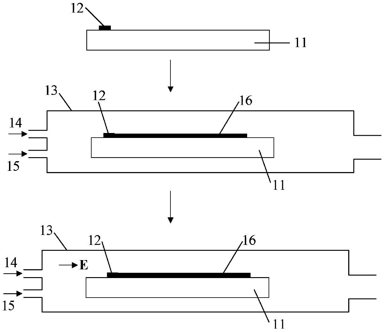
[0031] see figure 1 , the first embodiment of the present invention provides a method for preparing carbon nanotubes, which includes the following steps:

[0032] Step S11, providing a substrate 11, depositing a catalyst layer 12 on the surface of the substrate 11;

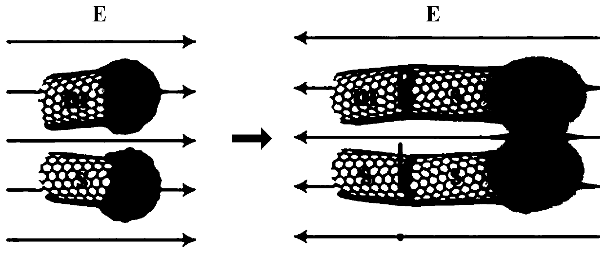
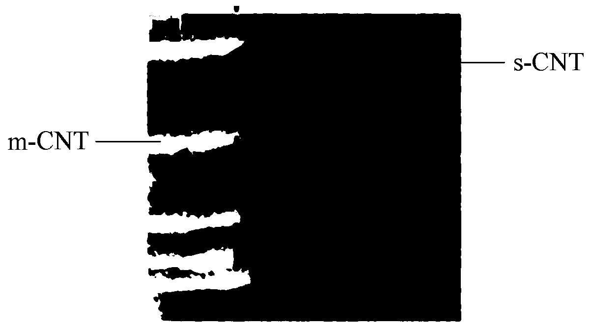
[0033] Step S12, setting the substrate 11 in a reaction furnace 13, heating to make the temperature in the reaction furnace reach a predetermined temperature, passing a carbon source gas 14 and a protective gas 15 into the reaction furnace 13, so that the substrate 11 Growing a carbon nanotube segment structure 16, the carbon nanotube segment structure 16 inc...


PUM

PropertyMeasurementUnit
diameteraaaaaaaaaa
diameteraaaaaaaaaa
diameteraaaaaaaaaa

Abstract

The invention relates to a thin film transistor, which comprises: an insulating substrate; a gate, the gate is arranged on the surface of the insulating substrate; a gate insulating layer, the gate insulating layer is arranged on the gate A surface away from the insulating substrate; a carbon nanotube structure, the carbon nanotube structure is disposed on the surface of the gate insulating layer away from the grid; wherein, the carbon nanotube structure includes at least one carbon nanotube, the carbon nanotube It includes a semiconducting carbon nanotube segment and two metallic carbon nanotube segments respectively connected to the two ends of the semiconducting carbon nanotube segment, and the two metallic carbon nanotube segments serve as source and drain respectively, the Semiconducting carbon nanotube segments serve as channels.

Description

technical field [0001] The invention relates to the technical field of carbon nanotubes, in particular to a thin film transistor prepared by using carbon nanotubes. Background technique [0002] Carbon nanotubes have attracted extensive attention due to their excellent properties such as high Young's modulus, tensile strength, and high thermal conductivity. [0003] In the single-walled carbon nanotubes prepared by the traditional chemical vapor deposition method, the ratio of metallic carbon nanotubes and semiconducting carbon nanotubes is about 1:2. In order to obtain semiconducting carbon nanotubes with higher purity, in the past two decades, after continuous research on the thermodynamics and kinetics of carbon nanotubes, people have been able to grow semiconducting carbon with a purity of 97% by CVD. nanotube. [0004] However, it is still not possible to directly grow semiconducting carbon nanotubes with higher purity. At the same time, in the prior art, the chirali...

Claims


Application Information

Patent Timeline
Patent Type & Authority Patents(China)
IPC IPC(8): H01L51/30H01L51/05H01L51/10B82Y30/00
CPCB82Y30/00H10K85/221H10K10/484H10K10/82B82Y10/00H10K10/466H01L29/786H01L29/4908B82Y40/00H01L29/41733
Inventor 王江涛柳鹏姜开利范守善
Owner TSINGHUA UNIV
Why Eureka
Try Eureka