Quantum dot light-emitting diode and application thereof
A quantum dot light-emitting and diode technology, which is applied in the manufacture of electrical components, electric solid devices, semiconductor/solid-state devices, etc., can solve problems such as the performance of quantum dot light-emitting diodes to be improved, reduce leakage current, reduce defects, and improve cost performance. The effect of membrane quality
- Summary
- Abstract
- Description
- Claims
- Application Information
AI Technical Summary
Problems solved by technology
Method used
Image
Examples
Embodiment 1
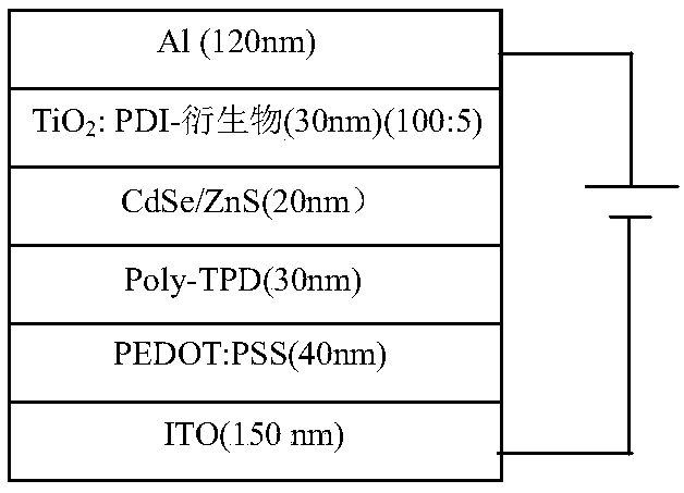
[0026] In this embodiment, a quantum dot light emitting diode has a structure such as figure 1 As shown, it includes a substrate (including the first electrode ITO), a hole injection layer (PEODT:PSS) laminated on the substrate, a hole transport layer (poly-TPD) laminated on the surface of the hole injection layer, and a hole injection layer (poly-TPD) laminated on the surface of the hole. The quantum dot luminescent layer (CdSe / ZnS) on the surface of the hole transport layer, the electron transport layer (TiO 2 : PDI-Py), and the second electrode (Al) disposed on the electron transport layer.
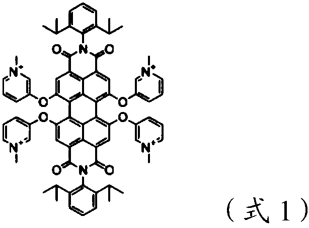
[0027] The material of the electron transport layer includes TiO with a diameter of 3 to 5 nm in a mass ratio of 100:5 2 Nanoparticles and peryleneimide derivatives (PDI-Py, see formula 1 for the structure).
[0028]
[0029] The preparation method of the above-mentioned quantum dot light-emitting diode is as follows:
[0030] (1) Substrate cleaning: The glass substrate with 150n...
Embodiment 2
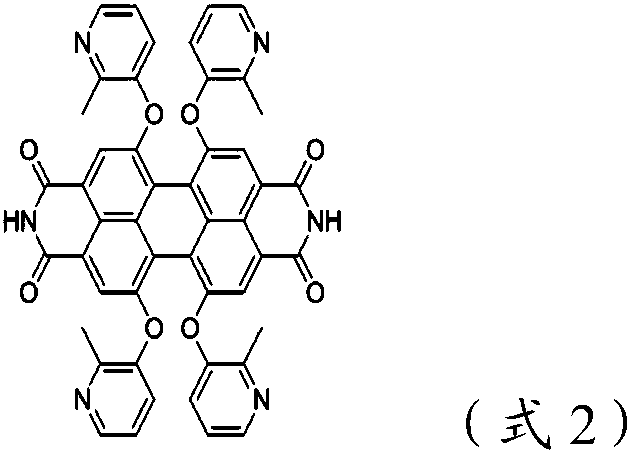
[0039] This embodiment is a kind of quantum dot light-emitting diode, its raw material and production method are similar to Embodiment 1, the difference is that: the material of the electron transport layer includes HfO with a diameter of 3 to 5 nm and a weight ratio of 100:5. 2 Nanoparticles and peryleneimide derivatives (see formula 2 for the structure).
[0040]
Embodiment 3
[0042] This embodiment is a kind of quantum dot light-emitting diode, its raw material and production method are similar to Embodiment 1, the difference is that: the material of the electron transport layer includes TiO with a diameter of 3 to 5 nm in a weight ratio of 100:1. 2 Nanoparticles and peryleneimide derivatives (see formula 1 for the structure).
[0043]
PUM
| Property | Measurement | Unit |
|---|---|---|
| particle diameter | aaaaa | aaaaa |
| thickness | aaaaa | aaaaa |
| thickness | aaaaa | aaaaa |
Abstract
Description
Claims
Application Information


