Laser power supply circuit board and preparation method thereof

A laser power supply and circuit board technology, which is applied in the manufacture of printed circuits, assembly of printed circuits with electrical components, printed circuits, etc., can solve problems such as circuit board damage and large circuit current

Inactive Publication Date: 2018-12-07
临沂朝日电子有限公司
View PDF5 Cites 0 Cited by
  • Summary
  • Abstract
  • Description
  • Claims
  • Application Information

AI Technical Summary

Problems solved by technology

[0003] In order to solve the problem in the prior art that part of the circuit in the circuit board has a large current and the circuit board is easily damaged due to excessive heat, the present invention provides a laser power supply circuit board with a large load current

Method used


Image

  • Laser power supply circuit board and preparation method thereof

Examples


Embodiment 1

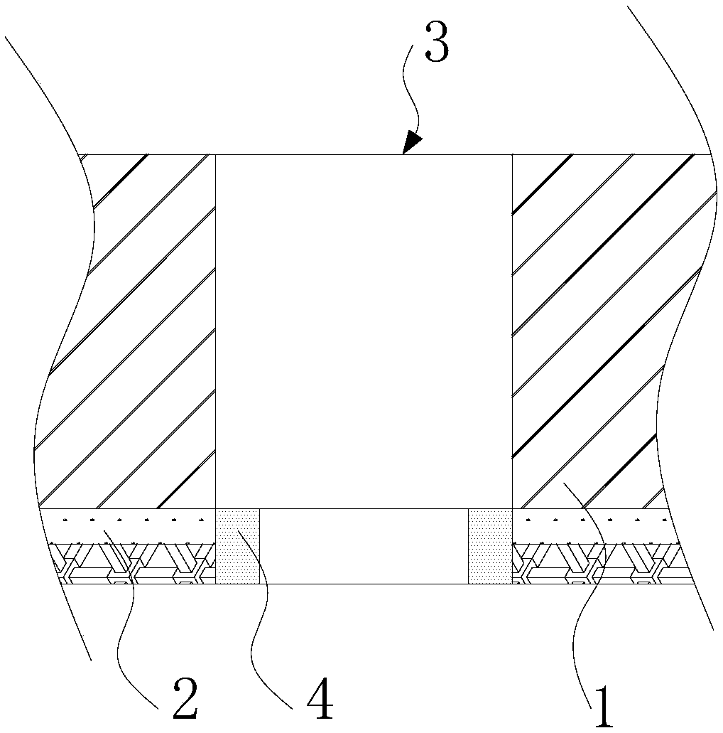
[0020] A laser power supply circuit board provided in this embodiment, such as figure 1 As shown, the circuit of the PCB board is provided with solder holes 3 and mounting holes for installing components. The solder hole is arranged in the circuit part with relatively large current, the inner diameter of the pad 4 of the solder hole 3 is 40-46mil, the inner diameter of the solder hole 3 is 55-65mil, and the solder hole 3 is filled with solder.

[0021] Further, the solder in the solder hole 3 is filled during wave soldering of each component.

[0022] Further, the inner diameter of the pad 4 of the solder hole 3 is 42-44mil, and the inner diameter of the solder hole 3 is 58-62mil.

[0023] The above-mentioned laser power supply circuit board is provided with a solder hole 3 on the circuit of the PCB board, and the solder hole 3 is filled with solder. The current flow path in the circuit is as follows: the copper skin 2 formed by sinking copper in the circuit, the solder pad 4...

Embodiment 2

[0025] The present invention also provides a method for preparing a laser power circuit board. When preparing a bare PCB, in addition to providing mounting holes for installing components, solder holes 3 are also provided on the circuit. The inner diameter of the pad 4 of the solder hole 3 is 40-46mil, and the inner diameter of the solder hole 3 is 55-65mil. When preparing the laser power circuit board, first insert the components into the mounting holes, and then solder the components by wave soldering.

[0026] In the laser power supply circuit board prepared by the above method, the circuit part with the solder hole 3 has a large current flow channel and a small resistance; it can prevent the circuit from being damaged by heat due to excessive current. The solder holes 3 are set on the circuit board in advance, and the solder holes 3 are filled with solder when the components are soldered by wave soldering. There is no need to pay other labor for filling the solder, and the...


PUM


Abstract

The invention provides a laser power supply circuit board and a preparation method thereof. The circuit of a PCB bare board is provided with a soldering tin hole and mounting holes for mounting components. The soldering tin hole is internally provided with a pad. In preparation of the laser power supply circuit board, components are inserted into the mounting holes, and then the components are welded in a wave soldering manner. The soldering tin hole of the prepared laser power supply circuit board is filled with soldering tin. According to the laser power supply circuit board prepared according to the preparation method, the soldering tin hole is filled with the soldering tin; and the circuit part with the soldering tin hole has a large current flowing channel and small resistance, and therefore damage of the circuit caused by overheat because of overhigh current can be prevented. The soldering tin hole is arranged on the circuit board in advance, and the soldering tin is applied to the soldering tin hole in soldering each component through wave soldering, thereby realizing no requirement for other labor for filling the soldering tin hole, and realizing simple and convenient manufacturing process of the laser power supply circuit board.

Description

technical field [0001] The invention relates to a circuit board and a preparation method thereof, in particular to a laser power supply circuit board which is not easy to burn out when the current and voltage are large, and a preparation method thereof. Background technique [0002] In the existing circuit boards, the components are mostly inserted into the mounting holes first, and then the components are soldered on the circuit board by wave soldering. However, for some circuit boards, especially the laser power supply circuit board, some circuits on the circuit board pass a large current, and the circuit board is prone to heat and burn. Contents of the invention [0003] In order to solve the problem in the prior art that part of the circuit in the circuit board has a large current and the circuit board is easily damaged due to excessive heat, the present invention provides a laser power supply circuit board with a large load current. [0004] The invention provides a ...

Claims


Application Information

Patent Timeline
IPC IPC(8): H05K1/02H05K3/34H05K3/42
CPCH05K1/0265H05K3/3447H05K3/42H05K2201/09563
Inventor 朱中林
Owner 临沂朝日电子有限公司
Why Eureka
Try Eureka