Preparation method of white light chip

A chip and white light technology, applied in the direction of electrical components, electric solid devices, circuits, etc., can solve the problems such as the utilization rate of light has not been effectively improved, with yellow or blue light spots, LED chips can not reach, etc., to achieve luminous Small angle, low cost, uniform spot effect

Inactive Publication Date: 2018-12-11
LATTICE POWER (JIANGXI) CORP
View PDF5 Cites 6 Cited by
  • Summary
  • Abstract
  • Description
  • Claims
  • Application Information

AI Technical Summary

Problems solved by technology

[0003] At present, the preparation of white light LED is mainly made by coating yellow phosphor powder on the blue light chip, that is, directly coating or spraying a layer of phosphor powder glue on the surface of the blue light LED chip, and the white light LED chip prepared according to the above process exists as follows Two problems: one is that only a layer of phosphor glue is coated on the surface of the blue LED chip, but the side of the chip is not coated with phosphor glue, so there will be blue light leakage around the chip, resulting in the white light color of the final packaged white LED device. Uneven, often with yellow or blue spots; Second, the white LED chip prepared by the above method emits light from five sides, and most of the side light becomes ineffective light, and the utilization rate of light has not been effectively improved
In addition, in some application fields that require LED products to have the characteristics of miniaturization, integration, and smaller lighting angles, such as flashlights, TV backlights, etc., LED chips prepared by traditional methods cannot meet the requirements of these fields.

Method used


Image

  • Preparation method of white light chip
  • Preparation method of white light chip
  • Preparation method of white light chip

Examples


Embodiment Construction

[0021] This embodiment adopts the following steps:

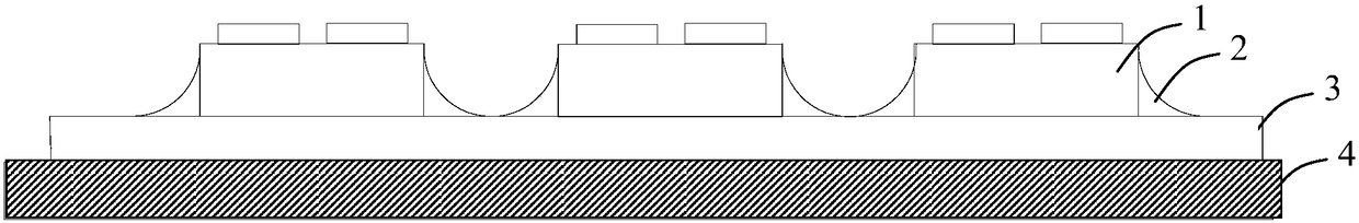
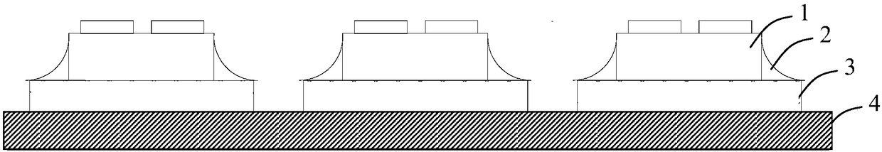
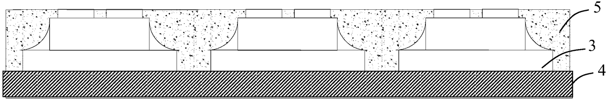
[0022] Prepare and select a fluorescent film 3 that meets the requirements, and electroplate metal on the electrode of the flip-chip blue LED chip 1 as a metal electrode. Place the fluorescent film 3 on the support substrate 4, and then dot transparent silica gel on the surface of the fluorescent film 3 according to preset rules, such as uniformly spot transparent silica gel 2 of the same size on the surface of the fluorescent film 3; after that, prepare the metal electrode The flip-chip blue LED chip 1 (the surface on the side where the metal electrode is not prepared) is placed on the position of the transparent silica gel in the fluorescent film, and baked at a temperature of 150° for 2 hours, so that the surface around the flip-chip blue LED chip The transparent silica gel 2 presents a concave arc shape, such as figure 1 shown;

[0023] Cut the fluorescent film 3 along the cutting line, and expand the distance between...


PUM


Abstract

The invention provides a preparation method of a white light chip. The preparation method comprises the steps of placing a fluorescent membrane on a support substrate; dispensing transparent silica gel on the surface of the fluorescent thin film according to a preset rule; placing an inverted blue-ray LED chip on the surface of the transparent silica gel and solidifying; cutting the fluorescent membrane along a cutting path; filling high-reflection glue between every two adjacent LED chips and solidifying; cutting along the grooves between the adjacent LED chips to obtain a single white lightchip. The white light emitted by the white light LED chip is uniform in color, the phenomenon of blue light leakage is avoided, the light emitting efficiency is high, and the light emitting angle is small.

Description

technical field [0001] The invention relates to the field of semiconductor light emitting diodes, in particular to a method for preparing a white light chip. Background technique [0002] LED (Light Emitting Diode, Light Emitting Diode) is a solid-state semiconductor device that can convert electrical energy into visible light. Light, thus directly converting electrical energy into light energy. LED, especially white LED, is widely used as a new lighting source material. It has the advantages of fast response, good shock resistance, long life, energy saving and environmental protection, etc. and has developed rapidly. It has been widely used in landscaping and Indoor and outdoor lighting and other fields. [0003] At present, the preparation of white light LED is mainly made by coating yellow phosphor powder on the blue light chip, that is, directly coating or spraying a layer of phosphor powder glue on the surface of the blue light LED chip, and the white light LED chip p...

Claims


Application Information

Patent Timeline
Patent Type & Authority Applications(China)
IPC IPC(8): H01L33/48H01L33/50H01L33/60H01L33/62H01L25/075
Inventor 肖伟民朴一雨李珍珍徐海丁小军
Owner LATTICE POWER (JIANGXI) CORP
Why Eureka
Try Eureka