Asymmetric van der Waals heterojunction device, preparation method and use thereof

A heterojunction, asymmetric technology, applied in the direction of electric solid devices, semiconductor devices, electrical components, etc., to achieve the effect of high responsivity

Active Publication Date: 2018-12-14
THE NAT CENT FOR NANOSCI & TECH NCNST OF CHINA
View PDF9 Cites 12 Cited by
  • Summary
  • Abstract
  • Description
  • Claims
  • Application Information

AI Technical Summary

Problems solved by technology

A van der Waals heterojunction device capable of achieving sufficient performance in multiple functions simultaneously has not yet been reported

Method used


Image

  • Asymmetric van der Waals heterojunction device, preparation method and use thereof
  • Asymmetric van der Waals heterojunction device, preparation method and use thereof
  • Asymmetric van der Waals heterojunction device, preparation method and use thereof

Examples


Embodiment 1

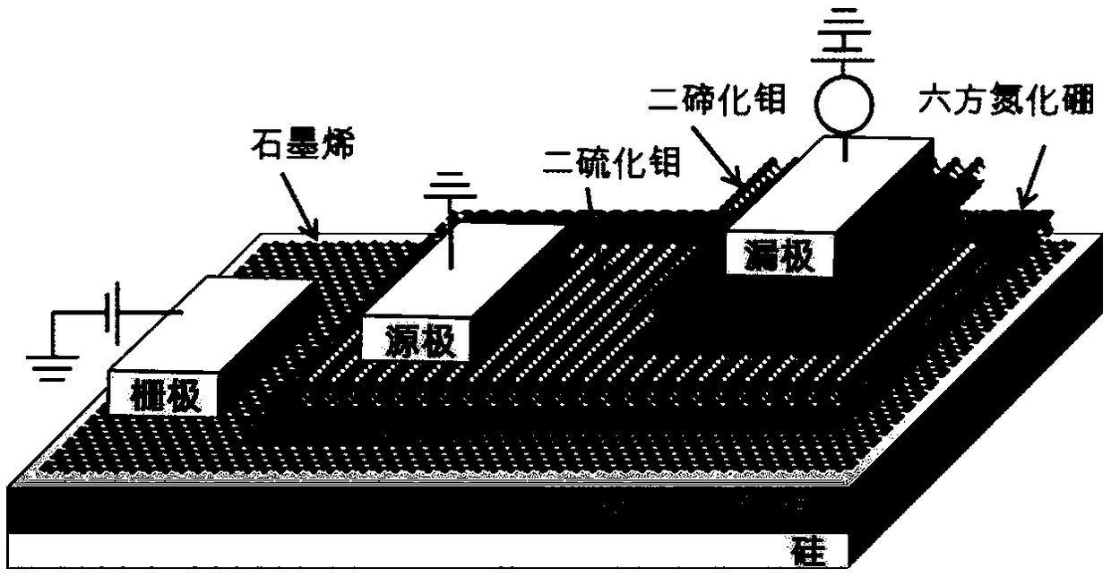
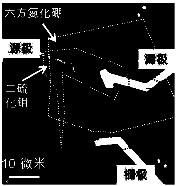
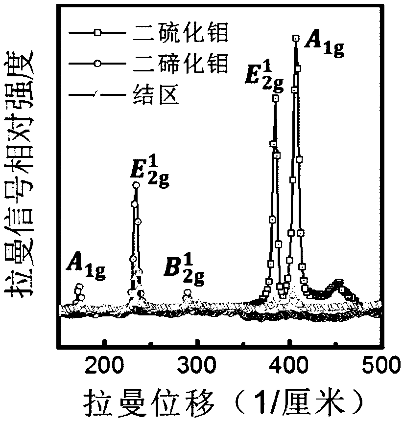
[0041]Fabrication of Asymmetric Van der Waals Heterojunction Devices.

[0042] (1) Graphene nanosheets, hexagonal boron nitride nanosheets, molybdenum disulfide nanosheets, and molybdenum ditelluride nanosheets were all prepared by pasting corresponding bulk materials repeatedly with scotch tape. With the aid of optical microscopy, single-layer graphene nanosheets on scotch tape were placed directly on silicon substrates with 300 nm thick silica; hexagonal boron nitride nanosheets with a suitable thickness , molybdenum disulfide nanosheets and molybdenum ditelluride nanosheets were respectively transferred to a PPC (polymethylethylene carbonate) plastic support film with a thickness of about 300 nanometers. The thickness and area of ​​the corresponding nanosheets were selected by optical microscopy and atomic force microscopy. The thicknesses of the hexagonal boron nitride nanosheets, molybdenum disulfide nanosheets and molybdenum ditelluride nanosheets in Example 1 are 13.8 ...

Embodiment 2

[0055] Fabrication of Asymmetric Van der Waals Heterojunction Devices:

[0056] (1) Graphene nanosheets, hexagonal boron nitride nanosheets, molybdenum disulfide nanosheets, and molybdenum ditelluride nanosheets were all prepared by pasting corresponding bulk materials repeatedly with scotch tape. With the aid of optical microscopy, single-layer graphene nanosheets on scotch tape were placed directly on silicon substrates with 300 nm thick silica; hexagonal boron nitride nanosheets with a suitable thickness , molybdenum disulfide nanosheets and molybdenum ditelluride nanosheets were respectively transferred to a PPC (polymethylethylene carbonate) plastic support film with a thickness of about 300 nanometers. The thickness and area of ​​the corresponding nanosheets were selected by optical microscopy and atomic force microscopy. The thicknesses of the hexagonal boron nitride nanosheets, molybdenum disulfide nanosheets, and molybdenum ditelluride nanosheets in Experimental Exam...


PUM

PropertyMeasurementUnit
thicknessaaaaaaaaaa
thicknessaaaaaaaaaa
thicknessaaaaaaaaaa

Abstract

The invention provides an asymmetric van der Waals heterojunction device, comprising graphene nanosheets, hexagonal boron nitride nanosheets, molybdenum disulfide nanosheets and molybdenum telluride nanosheets sequentially arranged from bottom to top; The graphene nano sheet and the hexagonal boron nitride nano sheet, the molybdenum disulfide nano sheet and the molybdenum telluride nano sheet havean overlapping region; A surface area of that molybdenum disulfide nanosheet is lar than that of the molybdenum telluride nanosheet, and parts of the molybdenum disulfide nanosheet do not overlap with the molybdenum telluride nanosheet. The invention also provides the preparation and application of the asymmetric van der Waals heterojunction device. The asymmetric van der Waals heterojunction device of the invention can realize the organic unity of ultra high performance and multiple functions. When operating as a transistor, the device exhibits ultra-high current switching ratio, ultra-smallsubthreshold swing and obvious negative transconductance behavior. When operating as a rectifier, the device exhibits an ultra-high current rectification ratio. When operating as memory, the device exhibits an ultra-high erase/write current ratio and current rectification ratio.

Description

technical field [0001] The invention belongs to the technical field of semiconductor materials, and in particular relates to an asymmetric van der Waals heterojunction device and its preparation and application. Background technique [0002] Due to their novel properties and high compatibility with silicon-based technologies, 2D layered materials show great promise in fields such as field-effect transistors, memories, and photodetectors. More importantly, these ultrathin 2D materials can be freely assembled by van der Waals forces to form ultrathin van der Waals heterojunctions. By selecting two-dimensional materials with different properties and specific assembly methods, their unique functions can be organically combined. From this research point of view, van der Waals heterojunction provides us with a new platform to study the properties of novel electronic and optoelectronic devices. [0003] Currently, research on high-performance van der Waals heterojunctions is larg...

Claims


Application Information

Patent Timeline
Patent Type & Authority Applications(China)
IPC IPC(8): H01L29/06H01L31/109H01L27/115
CPCH01L29/0665H01L29/0684H01L31/109H10B69/00
Inventor 何军程瑞清王峰
Owner THE NAT CENT FOR NANOSCI & TECH NCNST OF CHINA
Why Eureka
Try Eureka