N-type high-efficiency crystalline silicon solar cell and preparation method thereof

A technology of solar cells and crystalline silicon, applied in the field of solar cells, can solve the problems of low doping efficiency and carrier mobility of amorphous silicon films, achieve the effects of improving electrical characteristics, low equipment cost, and improving conversion efficiency

Inactive Publication Date: 2018-12-14
JIANGSU SHUNFENG PHOTOVOLTAIC TECH CO LTD
View PDF0 Cites 3 Cited by
  • Summary
  • Abstract
  • Description
  • Claims
  • Application Information

AI Technical Summary

Problems solved by technology

[0005] Aiming at the defects of relatively low doping efficiency and carrier mobility of the current amorphous silicon thin film, the present invention proposes an N-type high-efficiency crystalline silicon solar cell and its preparation method, which can operate at a relatively low temperature (250-300 degrees) Grow polycrystalline silicon germanium thin films under conditions, and achieve N-type and P-type in-situ doping, effectively improve the electrical characteristics of the cell emitter and back field materials, and further improve the conversion efficiency of solar cells

Method used


Image

  • N-type high-efficiency crystalline silicon solar cell and preparation method thereof

Examples


Embodiment

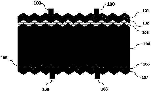
[0025] Embodiment: the present invention provides a kind of N-type high-efficiency crystalline silicon solar cell and preparation method thereof, such as figure 1 As shown, its structure includes a front surface metal electrode 100, a front surface ITO film 101, a boron-doped polycrystalline silicon germanium film (emitter) 102, a front surface intrinsic amorphous silicon film 103, an N-type crystalline silicon 104, and a back surface intrinsic An amorphous silicon film 105 , a phosphorus-doped polycrystalline silicon germanium film (back field) 106 , an ITO film 107 on the back surface, and a metal electrode 108 on the back surface.

[0026] The specific steps of the preparation method of the present invention are as follows:

[0027] Firstly, conventional texturing is performed on N-type crystalline silicon, and textured structures appear on both the front surface and the back surface of the crystalline silicon substrate after texturing. Next, perform standard RCA cleaning ...


PUM

PropertyMeasurementUnit
thicknessaaaaaaaaaa
thicknessaaaaaaaaaa

Abstract

The invention relates to an N-type high-efficiency crystalline silicon solar cell and a preparation method thereof. The structure comprises a front metal gate line, a front ITO film, a front boron-doped polysilicon germanium film, a front intrinsic amorphous silicon film, an N-type crystalline silicon substrate, a back intrinsic amorphous silicon film, a back phosphorus-doped polysilicon germaniumfilm, a back ITO film and a back metal gate line. The structure comprises a front metal gate line, a front ITO film, a front boron-doped polysilicon germanium film, a front intrinsic amorphous silicon film, an N-type crystalline silicon substrate, a back amorphous silicon film, a back phosphorus doped polysilicon germanium film, a back ITO film and a back metal gate line. A method for manufacturethat N-type crystal silicon wafer comprise the steps of double-sided velvet making of the N-type crystal silicon wafer, Then P-type polysilicon germanium thin film and N-type polysilicon germanium thin film are prepared on the front and back surface of crystalline silicon as emitter and back field, respectively. Then ITO transparent conductive thin film is prepared on both sides. Finally, metal gate line electrodes are prepared on the front and back surface of the cell. The invention obtains the polycrystalline silicon germanium thin film with high doping efficiency under the condition that the process temperature does not exceed 300oC and the intrinsic passivation performance of the amorphous silicon thin film is not damaged, and further improves the conversion efficiency of the battery.

Description

technical field [0001] The invention belongs to the field of solar cells, and in particular relates to a structural design and a preparation method of an N-type high-efficiency crystalline silicon solar cell. Background technique [0002] The rapid development of the photovoltaic industry requires an industrialized technology with simple process flow and higher photoelectric conversion efficiency to reduce the cost of power generation and achieve the goal of the same price as the mains electricity or even lower than the mains electricity price. [0003] With the development of industrialization, the current conventional crystalline silicon solar cells have made great progress in various aspects such as improvement of conversion efficiency and cost reduction, but their structure and technical characteristics limit the further improvement of their efficiency. Therefore, a variety of solutions have emerged in the industry, including selective emitter solar cells, back-junction ...

Claims


Application Information

Patent Timeline
Patent Type & Authority Applications(China)
IPC IPC(8): H01L31/028H01L31/0368H01L31/076H01L31/18
CPCH01L31/028H01L31/03687H01L31/076H01L31/1804Y02E10/547Y02E10/548Y02P70/50
Inventor 贾锐陶科孙恒超瞿辉徐春曹玉甲汤佳丽刘斌陈必华周颖
Owner JIANGSU SHUNFENG PHOTOVOLTAIC TECH CO LTD
Why Eureka
Try Eureka