Resistance value measurement circuit device and method for semiconductor memory
A technology of circuit device and resistance value, which is applied in the field of resistance value measurement circuit device of semiconductor memory, to achieve the effect of avoiding influence and avoiding contact resistance
- Summary
- Abstract
- Description
- Claims
- Application Information
AI Technical Summary
Problems solved by technology
Method used
Image
Examples
Embodiment 1
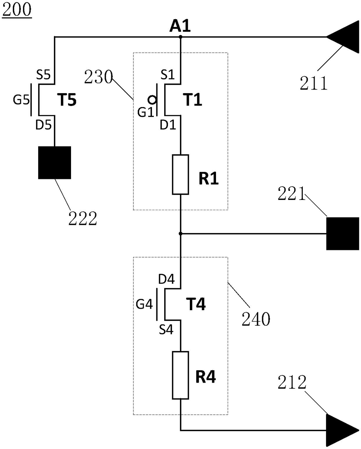
[0093] Such as figure 2 As shown, the resistance value measurement circuit device 200 of this embodiment includes a first calibrated unit 230, a first protection unit 240, and a first measurement switch transistor T5. By measuring the resistance value of the first calibrated unit 230, further Calibrate the resistance value of the first calibrated unit 230 .
[0094] The first unit to be calibrated 230 is connected between the first voltage interface 211 and the first reading interface 221, and the first connection point A1 is formed at the place where the first unit to be calibrated 230 is connected to the first voltage interface 211 The first measurement switching transistor T5 is connected between the first connection point A1 and the second read interface 222 ; the first protection unit 240 is connected between the second voltage interface 212 and the first read interface 221 .
[0095] Preferably, the first measurement switch transistor T5 is an N-type metal oxide semico...
Embodiment 2
[0113] Such as Figure 4 As shown, this embodiment provides a measurement circuit 300 for a semiconductor memory. The difference from Embodiment 1 is that a second calibrated unit 350, a second protection unit 360 and a second measurement switching transistor T6 are added, and the throughput The resistance value of the second unit to be calibrated 350 is measured, and then the resistance value of the second unit to be calibrated 360 is calibrated.
[0114] The second unit to be calibrated 350 is connected between the second voltage interface 212 and the first reading interface 221, and the second connection point A2 is formed at the place where the second unit to be calibrated 350 is connected to the second voltage interface 212 The second measurement switch transistor T6 is connected between the second connection point A2 and the third read interface 323 ; the second protection unit 360 is connected between the first voltage interface 211 and the first read interface 221 .
...
Embodiment 3
[0136] This embodiment provides a method for measuring the resistance of a semiconductor memory, which can be based on the resistance measuring circuit device 300 described above.
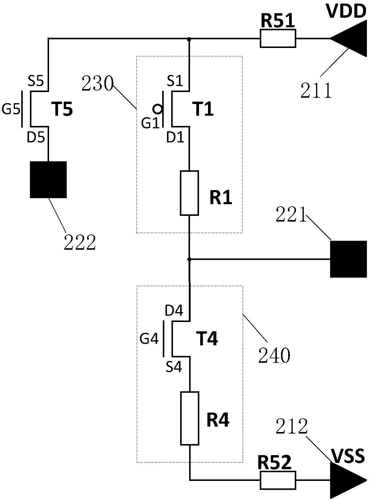
[0137] Such as Figure 6 As shown, a voltage difference is provided between the first voltage interface 211 and the second voltage interface 212 , for example, the operating voltage VDD is applied to the first voltage interface 211 , and the ground voltage VSS is applied to the second voltage interface 212 .
[0138] Wherein, the working voltage VDD and the grounding voltage VSS may come from the interface card of the testing machine.
[0139] Turn on the first measurement switch transistor T5 and turn on the second measurement switch transistor T6. It should be noted that the first measurement switch transistor T5 and the second measurement switch transistor T6 may not always be turned on. When measuring the first calibrated unit 230, the first measurement switch transistor T5 is turned on and th...
PUM
 Abstract
Description
Claims
Application Information


