Narrow-band optical filter and all-optical diode

An all-optical diode and filter technology, applied in light guides, optics, instruments, etc., can solve problems such as not meeting application requirements, and achieve the effect of simple structure, flexible and adjustable parameters, and small size

Inactive Publication Date: 2018-12-18
CHINA UNIV OF GEOSCIENCES (BEIJING)
View PDF10 Cites 15 Cited by
  • Summary
  • Abstract
  • Description
  • Claims
  • Application Information

AI Technical Summary

Problems solved by technology

[0003] At present, all-optical diodes can be realized based on the magneto-optic effect, optical nonlinear effect, and space-time modulation technology. The optical nonlinear effect and the space-time modulation technology that needs to be modulated by an external electric field do not meet the application requirements

Method used


Image

  • Narrow-band optical filter and all-optical diode
  • Narrow-band optical filter and all-optical diode
  • Narrow-band optical filter and all-optical diode

Examples


Embodiment 1

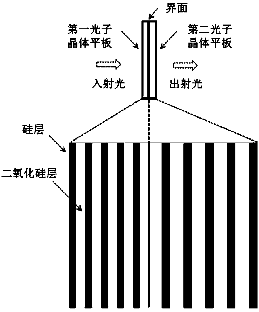
[0033] Embodiment 1: as figure 1 As shown, the narrow-band optical filter proposed by the present invention includes:

[0034] The first photonic crystal plate and the second photonic crystal plate; wherein,

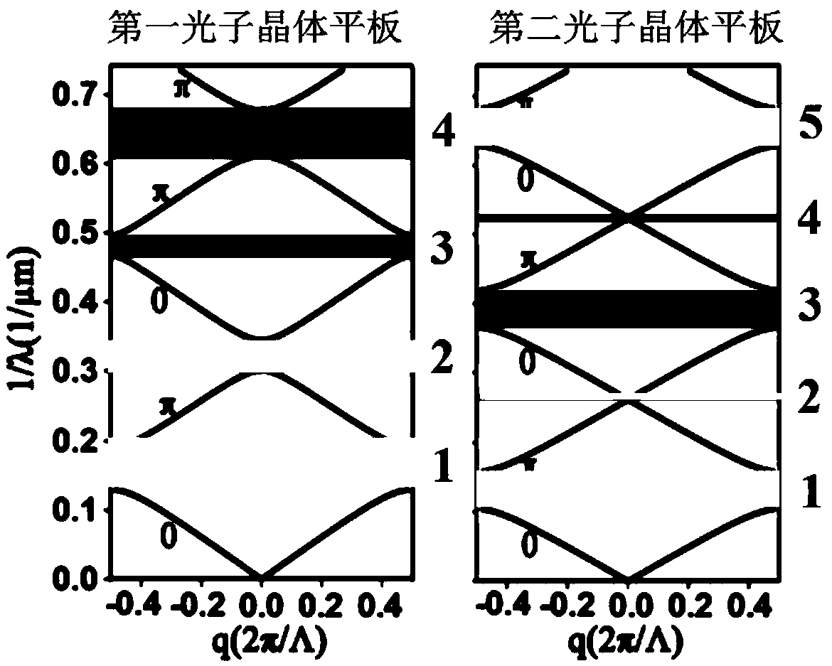
[0035] The first and second photonic crystal slabs are one-dimensional photonic crystals composed of alternately stacked silicon layers and silicon dioxide layers with uniform thickness. and topologically opposite bandgap;

[0036] The first and second photonic crystal plates are bonded together to form a one-dimensional photonic crystal heterostructure;

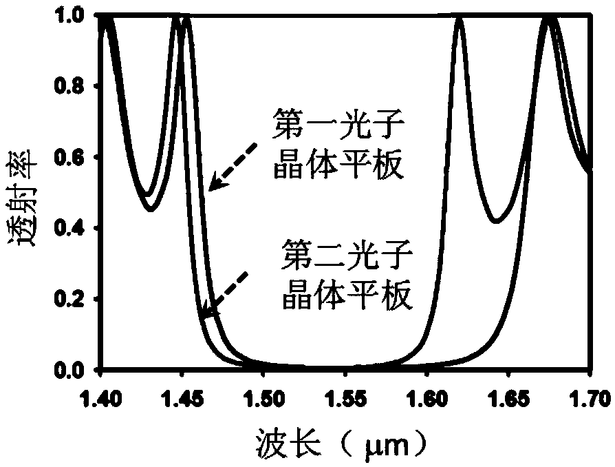
[0037] The above energy band structures of the first and second photonic crystal slabs make the one-dimensional photonic crystal heterostructure satisfy the conditions for exciting the optical topological interface state and excite the optical topological interface state in the common band gap of the first and second photonic crystal slabs, showing In order to have a sharp transmission peak in the common band gap of...

Embodiment 2

[0052] Embodiment 2: as Figure 6 As shown, the all-optical diode proposed by the present invention includes:

[0053] The photonic crystal heterostructure in embodiment 1, and the planar grating;

[0054] Wherein, the planar grating is a one-dimensional planar grating made of silicon material, and the direction of its period is perpendicular to the period direction of the first and second photonic crystal plates in Embodiment 1;

[0055] The planar grating is attached to the second photonic crystal plate in Embodiment 1, and is used to control the excitation of the topological interface state based on its diffraction effect on light, so as to realize the unidirectional transmission of light.

[0056] In this embodiment, the plane grating changes the excitation condition of the interface state through its diffraction effect on light. When the incident light is incident from one side of the planar grating, the incident light will be diffracted to many directions. At this time...


PUM


Abstract

The invention discloses a narrow-band optical filter and an all-optical diode. The narrow-band optical filter comprises first and second photonic crystal panels; the first and second photonic crystalpanels are one-dimensional photonic crystal which is composed by alternately placed silicon layers and silicon dioxide layers in uniform thickness; the first and second photonic crystal panels are adhered together to compose a one-dimensional photonic crystal heterojunction which meets an optical topological interface state excitation condition; the excitation of the optical topological interfacestate shows that sharp transmission peaks appears in a common band gap of the first and second photonic crystal panels, the transmission ratio of two lateral bands is still zero and a narrow-band filtering function is accordingly realized; the central wavelength of the transmission peak is the working wavelength of the optical filter, and the bandwidth is the working bandwidth of the optical filter. The all-optical diode comprises the filter and the plane grating, and the plane grating is adhered to one end of the photonic crystal heterojunction structure. The grating is used for controlling the excitation of the topological interface state based on the diffraction thereof for the light, and single-direction transmission of the light is accordingly realized.

Description

technical field [0001] The invention relates to optical filtering technology and one-way transmission technology, in particular to a narrow-band optical filter and an all-optical diode, and belongs to the fields of optical communication and optical computing. Background technique [0002] All-optical diodes break the time-reversal symmetry of light transmission by using special optical materials or by means of specific optical effects, so that light signals pass in one direction, but rarely or basically do not pass in the opposite direction, similar to Electrical diodes in integrated circuits are key components for optical computing, optical interconnection, and ultrafast information processing. [0003] At present, all-optical diodes can be realized based on the magneto-optic effect, optical nonlinear effect, and space-time modulation technology. Neither the optical nonlinear effect nor the space-time modulation technology that needs to be modulated by an external electric...

Claims


Application Information

Patent Timeline
Patent Type & Authority Applications(China)
IPC IPC(8): G02B6/122
CPCG02B6/1225G02B2006/12107G02B2006/1213
Inventor 高华魏果果董鹏
Owner CHINA UNIV OF GEOSCIENCES (BEIJING)
Why Eureka
Try Eureka