A superjunction IGBT with a shielded gate and a manufacturing method thereof

A shielding gate and gate technology, which is applied in semiconductor/solid-state device manufacturing, electrical components, circuits, etc., can solve the problems of increasingly higher and higher requirements for the reduction range, and achieve higher turn-on and turn-off speeds , Improve the extraction speed and reduce the effect of switching loss

Pending Publication Date: 2018-12-18
无锡市乾野微纳科技有限公司
View PDF5 Cites 13 Cited by
  • Summary
  • Abstract
  • Description
  • Claims
  • Application Information

AI Technical Summary

Problems solved by technology

[0004] However, although super-junction IGBTs have been greatly improved in terms of conduction voltage drop, etc., as the application requirements become higher and higher, the requirements for reducing the conduction voltage drop Vce and switching loss Eoff are getting higher and higher. At the same time, the requirements for the short-circuit safe working area are getting higher and higher, and the existing IGBT devices are also facing more and more challenges. Therefore, how to further reduce the conduction voltage drop and switching loss of the IGBT device, and at the same time further improve the short-circuit withstand time Tsc has become an important issue. Important research directions for technicians in the technical field

Method used


Image

  • A superjunction IGBT with a shielded gate and a manufacturing method thereof
  • A superjunction IGBT with a shielded gate and a manufacturing method thereof
  • A superjunction IGBT with a shielded gate and a manufacturing method thereof

Examples


Embodiment 2

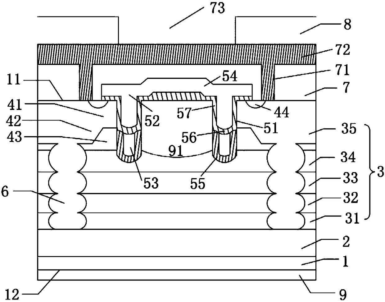
[0066] combine Figure 1 to Figure 12 As shown, this implementation provides a method for manufacturing a super-junction IGBT with a shielded gate, which is used to manufacture the super-junction IGBT described in Embodiment 1, including the following process steps:

[0067] S1. Provide a semiconductor substrate having a first main surface 11 and a second main surface 12, wherein P columns 6 are formed in the semiconductor substrate;

[0068] Wherein, step S1 specifically includes:

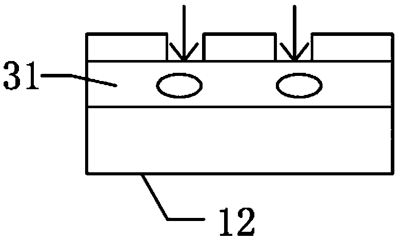
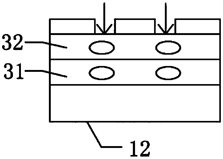
[0069] S111. Combine figure 1 with figure 2 As shown, a semiconductor substrate having a first epitaxial layer 31 of a first conductivity type and a second main surface 12 is provided, and the first epitaxial layer 31 of a first conductivity type and the second main surface 12 are arranged opposite to each other;

[0070] S112. Form a photoresist on the first epitaxial layer 31 of the first conductivity type, define the implantation region of the P column 6 by photolithography, inject impuriti...


PUM


Abstract

The invention discloses a superjunction IGBT with a shield gate and a manufacturing method thereof. The superjunction IGBT comprises a semiconductor substrate, a cell region and a terminal protectionarea. The semiconductor substrate comprises a second conductivity type collector region, a first conductivity type field termination layer and at least one first conductivity type epitaxial layer. Thecell region comprises a plurality of cells connected in parallel with each other, which includes a plurality of cell trenches and a gate conductive polysilicon and a shield gate filled in the cell trenches, A seventh oxide layer is arranged on both sides and sidewalls of the notch of the cell trench opposite to the gate conductive polysilicon, a fifth oxide layer is arranged between the gate conductive polysilicon and the shield gate, and a fourth oxide layer is arranged on the bottom and sidewalls of the cell trench opposite to the shield gate. A P-pillar is also provided in the first conductivity type epitaxial layer, one end of the P-pillar is connected to the second conductivity type well layer, and the other end extends toward the first conductivity type field termination layer. Theinvention adopts the shielding gate structure, reduces the Miller capacitance, thereby reducing the switching loss.

Description

technical field [0001] The invention relates to the technical field of power semiconductor devices, in particular to a super-junction IGBT with a shielded gate and a manufacturing method thereof. Background technique [0002] Insulated Gate Bipolar Transistor (IGBT) is a mainstream product in high-voltage and high-power power electronic devices. With the continuous upgrading of its structure, its application range is becoming wider and wider. The key parameters of IGBT include conduction voltage drop Vce, switching loss Eoff and short circuit withstand time Tsc. In practical applications, our goal is to obtain the lowest possible turn-on voltage drop Vce and switching loss Eoff, and a longer short-circuit withstand time Tsc. [0003] The introduction of super-junction technology in power devices has broken the contradiction between reducing the conduction voltage drop and improving the withstand voltage in traditional silicon devices. In super-junction IGBTs, the N-type bas...

Claims


Application Information

Patent Timeline
Patent Type & Authority Applications(China)
IPC IPC(8): H01L29/06H01L21/331H01L29/739
CPCH01L29/0634H01L29/66348H01L29/7393
Inventor 秦旭光吉炜
Owner 无锡市乾野微纳科技有限公司
Why Eureka
Try Eureka