Thin film transistor and preparation method thereof, and array substrate

A technology of thin-film transistors and metal layers, applied in semiconductor/solid-state device manufacturing, electrical solid-state devices, semiconductor devices, etc., can solve problems such as TFT electrical instability, passivation film faults, and lower product yields, and achieve improved contact Performance, avoid chamfering, improve the effect of electrical performance

Inactive Publication Date: 2018-12-18
SHENZHEN CHINA STAR OPTOELECTRONICS SEMICON DISPLAY TECH CO LTD
View PDF3 Cites 7 Cited by
  • Summary
  • Abstract
  • Description
  • Claims
  • Application Information

AI Technical Summary

Problems solved by technology

In the existing TFT manufacturing process, the first metal material layer and the second metal material layer with good adhesion are deposited on the active layer 5, and then etched by a photolithography process. The different metals are in the same etching solution and mutually In contact with or through other conductors, due to the different corrosion potentials, localized corrosion of the contact parts of the first metal material layer and the second metal material layer, that is, galvanic corrosion (galvanic corrosion), appears, and chamfering occurs, such as figure 1 As shown in the middle dotted line box, the appearance of chamfered corners is likely to cause subsequent faults in the passivation film, TFT electrical instability and other abnormalities, and even reduce product yield

Method used


Image

  • Thin film transistor and preparation method thereof, and array substrate
  • Thin film transistor and preparation method thereof, and array substrate
  • Thin film transistor and preparation method thereof, and array substrate

Examples


preparation example Construction

[0044] The present invention also provides a preparation method of a thin film transistor, the preparation method comprising the following steps:

[0045] providing a substrate;

[0046] forming a gate and a gate insulating layer on the substrate, and the gate insulating layer covers the gate;

[0047] forming a first metal layer on the gate insulating layer, the first metal layer including a first electrode and a second electrode disposed on the gate insulating layer at intervals;

[0048] An active layer and a second metal layer are formed on the first metal layer, the second metal layer includes a source electrode and a drain electrode arranged at intervals, one end of the active layer is sandwiched between the first electrode and the source electrode, and the active layer The other end of is sandwiched between the second electrode and the drain;

[0049] A passivation layer is deposited, and the passivation layer covers the exposed surfaces of the source electrode, the d...

Embodiment 1

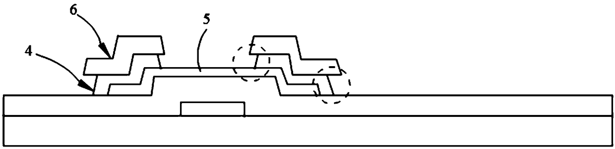
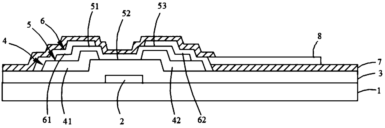
[0053] refer to figure 2 , the array substrate in this embodiment includes a plurality of thin film transistors 10, and the plurality of thin film transistors are arranged in an array. The thin film transistor 10 includes a substrate 1 , a gate 2 , a gate insulating layer 3 , a first metal layer 4 , an active layer 5 , a second metal layer 6 , and a passivation layer 7 . The gate 2 is arranged on the substrate 1, the gate insulating layer 3 covers the gate 2, the first metal layer 4 includes a first electrode 41 and a second electrode 42 arranged at intervals on the gate insulating layer 3, and the second metal layer 6 includes The source electrode 61 and the drain electrode 62 arranged at intervals, the source electrode 61 is located on the first electrode 41 and is in contact with the first electrode 41, the drain electrode 62 is located on the second electrode 42 and is in contact with the second electrode 42, and the active layer 5 includes The source contact end 51, the...

Embodiment 2

[0088] refer to Figure 8 The difference between this embodiment and Embodiment 1 is that the source 61 is not in contact with the first electrode 41 , and the drain 62 is not in contact with the second electrode 42 .

[0089] refer to Figures 9a-9j , the preparation method of the present embodiment adopts a half-tone mask process, and the preparation method comprises the steps of:

[0090] S1, provide a substrate 1, such as Figure 9a shown;

[0091] S2, form the gate 2 and the gate insulating layer 3 on the substrate 1, the gate insulating layer 3 covers the gate 2, such as Figure 9b shown;

[0092] S3, forming a first metal layer 4 on the gate insulating layer 3, the first metal layer 4 includes a first electrode 41 and a second electrode 42 arranged on the gate insulating layer 3 at intervals, such as Figure 9c shown;

[0093] S4, sequentially depositing the active material layer 50, the second metal material layer 60, and the third photoresist layer 70 on the first...


PUM


Abstract

A thin film transistor and a preparation method thereof and an array substrate are provided, the thin film transistor includes a substrate, a gate, a gate insulating layer, a first metal layer, an active layer, a second metal layer, and a passivation layer, the gate is disposed on the substrate, the gate insulating layer covers the gate, the first metal layer includes a first electrode and a second electrode spaced apart on the gate insulating layer, the second metal layer includes a source and a drain spaced apart, one end of the active layer is sandwiched between the first electrode and thesource electrode, the other end of the active layer is sandwiched between the second electrode and the drain electrode, and the passivation layer covers the exposed surfaces of the source electrode, the drain electrode and the active layer. By sandwiching the active layer between the first metal layer and the second metal layer, the contact performance between the active layer and the second metallayer is improved. In the preparation method of the present invention, the first metal layer and the second metal layer are formed by two times ofa composition process, thereby avoiding the occurrence of a chamfer.

Description

technical field [0001] The present invention relates to the technical field of array substrate manufacturing, in particular to a thin film transistor, a preparation method thereof, and an array substrate. Background technique [0002] Thin-film-transistor active-matrix liquid crystal display (TFTAMLCD) has become the leading technology and research and development hotspot in the field of information display because of its high information content, multi-gray scale and ability to realize color video display. With the development of TFTAMLCD to large area and high definition, the requirements for metal electrode materials are getting higher and higher. On the one hand, the resistance of the metal electrode is required to be low to reduce image distortion caused by signal delay; on the other hand, the thermal stability and adhesion of the metal film are better. Therefore, the preparation of metal thin films and circuits with low resistivity, good thermal stability and adhesion...

Claims


Application Information

Patent Timeline
Patent Type & Authority Applications(China)
IPC IPC(8): H01L29/861H01L21/336H01L27/12
CPCH01L27/1214H01L29/66742H01L29/861
Inventor 谢华飞陈书志
Owner SHENZHEN CHINA STAR OPTOELECTRONICS SEMICON DISPLAY TECH CO LTD
Why Eureka
Try Eureka