A BCD semiconductor device and a method for manufacture the same

A semiconductor and device technology, applied in the field of BCD devices and their manufacturing, which can solve the problems of limited application and rising on-resistance.

Active Publication Date: 2018-12-21
UNIV OF ELECTRONICS SCI & TECH OF CHINA
View PDF5 Cites 6 Cited by
  • Summary
  • Abstract
  • Description
  • Claims
  • Application Information

AI Technical Summary

Problems solved by technology

In a general power integrated chip, a high-voltage LDMOS device (Lateral Double-diffused MOSFET) is used as the output stage, but under a simple one-dimensional analysis, the specific on-resistance (Specificon-resistance, R on,sp ) and device breakdown voltage (Breakdown Voltage, BV) exist R on,sp ∝BV 2

Method used


Image

  • A BCD semiconductor device and a method for manufacture the same
  • A BCD semiconductor device and a method for manufacture the same
  • A BCD semiconductor device and a method for manufacture the same

Examples


Embodiment 1

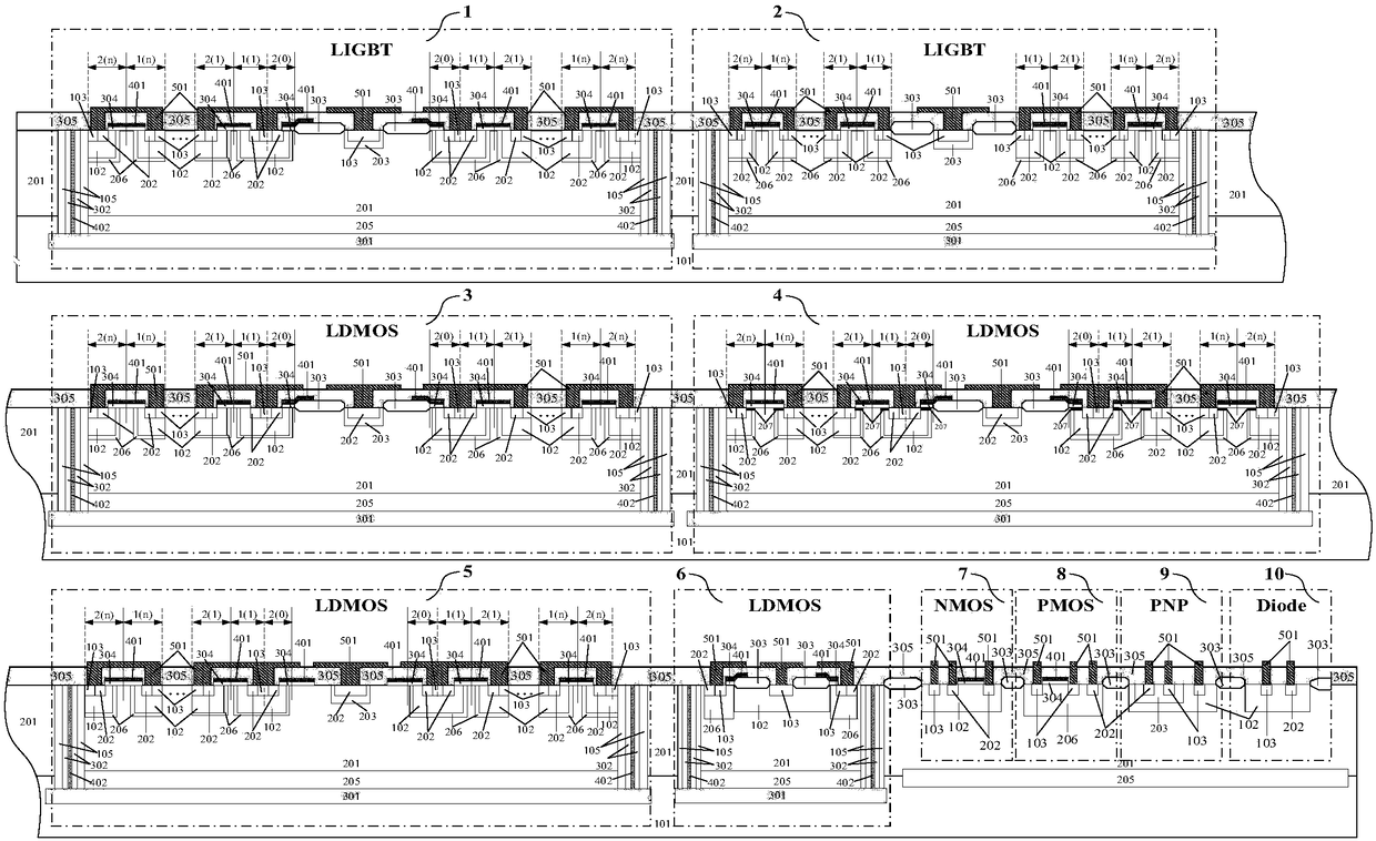
[0081] like figure 1 As shown, a BCD semiconductor device includes a first high-voltage nLIGBT device 1, a second high-voltage nLIGBT device 2, a first high-voltage nLDMOS device 3, a second high-voltage nLDMOS device 4, and a third high-voltage nLDMOS device 5 integrated on the same chip , the first high voltage pLDMOS device 6, the low voltage NMOS device 7, the low voltage PMOS device 8, the PNP device 9 and the diode device 10, the first high voltage nLIGBT device 1, the second high voltage nLIGBT device 2 and the first high voltage nLDMOS device 3, the first high voltage nLIGBT device 3, the first The second high-voltage nLDMOS device 4, the third high-voltage nLDMOS device 5, and the first high-voltage pLDMOS device 6 all adopt dielectric isolation to realize complete isolation of high-voltage and low-voltage devices. The first high-voltage nLIGBT device 1, the second high-voltage nLIGBT device 2, and the first high-voltage nLDMOS device 3. The second high-voltage nLDMOS...

Embodiment 2

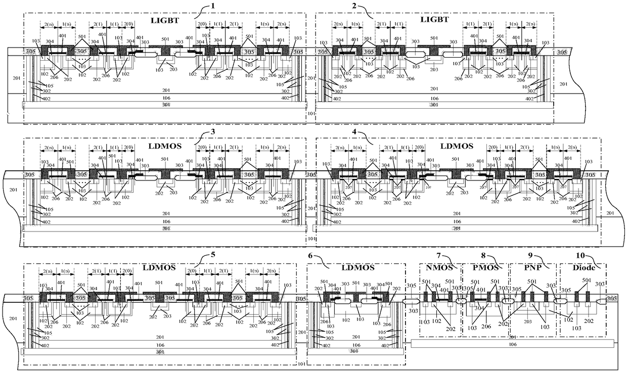
[0112] like figure 2 As shown, the difference between the BCD semiconductor device of this embodiment and Embodiment 1 lies in: the first high-voltage nLIGBT device 1, the second high-voltage nLIGBT device 2, the first high-voltage nLDMOS device 3, the second high-voltage nLDMOS device 4, and the first high-voltage nLDMOS device 4. Three high-voltage nLDMOS devices 5, the first high-voltage pLDMOS device 6, the buried layer 205 of the second conductivity type above the dielectric 301 is replaced with the first conductivity type withstand voltage structure 106, the first conductivity type withstand voltage structure 106 and the side wall of the dielectric groove 302 The implanted regions 105 of the first conductivity type are connected to each other.

Embodiment 3

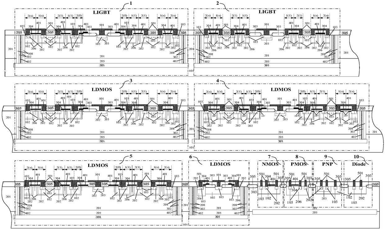
[0114] like image 3 As shown, the difference between the BCD semiconductor device of this embodiment and Embodiment 1 lies in: the first high-voltage nLIGBT device 1, the second high-voltage nLIGBT device 2, the first high-voltage nLDMOS device 3, the second high-voltage nLDMOS device 4, and the first high-voltage nLDMOS device 4. For the three high-voltage nLDMOS devices 5 and the first high-voltage pLDMOS device 6 , the left and right side walls of the dielectric trench 302 have the implanted regions 105 of the first conductivity type replaced with dielectric field-enhancing structures 208 of the second conductivity type.


PUM


Abstract

A BCD semiconductor device and a method for manufacture the same are provided, the BCD semiconductor device includes a first high voltage nLIGBT device, a second high voltage nLIGBT device, a first high voltage nLDMOS device, a second high voltage nLDMOS device, a third high voltage nLDMOS device, a first high voltage pLDMOS device, a Low Voltage NMOS Devices, a Low Voltage PMOS Devices, a PNP device and a diode device which are integrated on the same chip, wherein the High Voltage nLIGBT Device, the High Voltage nLDMOS Device, the High voltage pLDMOS device are dielectric isolated so as toa achieve complete isolation of high and low voltage devices. A nLIGBT, nLDMOS, Low Voltage NMOS, low voltage PMOS and low voltage NPN are are monolithically integrated on a substrate, The isolation region composed of dielectric, buried layer of second conductivity type, dielectric groove and injection region of first conductivity type realizes high and low voltage all-dielectric isolation on integrated chip, avoiding high and low voltage crosstalk problem. The multi-channel design is adopted in six types of high voltage tubes, which can effectively increase the current output capability of highvoltage tubes.

Description

technical field [0001] The invention belongs to the technical field of semiconductor power devices, and relates to a BCD (Bipolar CMOS DMOS) device and a manufacturing method thereof. Background technique [0002] High-voltage power integrated circuits often use the high analog precision of Bipolar transistors, the high integration of CMOS, and the high power or voltage characteristics of DMOS (Double-diffused MOSFET) to integrate Bipolar analog circuits, CMOS logic circuits, CMOS analog circuits and DMOS high-voltage power devices. Monolithically integrated together (referred to as BCD process). Lateral high-voltage devices are widely used in high-voltage power integrated circuits because the drain, gate, and source are all on the chip surface, and are easy to integrate with low-voltage signal circuits through internal connections. In a general power integrated chip, a high-voltage LDMOS device (Lateral Double-diffused MOSFET) is used as the output stage, but under a simpl...

Claims


Application Information

Patent Timeline
IPC IPC(8): H01L27/06H01L21/8249H01L27/02
CPCH01L21/8249H01L27/0274H01L27/0635H01L21/26533H01L21/76264H01L21/822H01L21/823878H01L27/0623H01L27/0629H01L27/0883H01L27/0922H01L27/1207H01L29/083H01L29/0856H01L29/0878H01L29/1083H01L29/42368H01L29/66325H01L29/66659H01L29/66681H01L29/735H01L29/7393H01L29/7824H01L29/7835H01L21/31155H01L21/324H01L21/76831H01L29/0649H01L29/0696H01L29/0808H01L29/0821H01L29/086H01L29/7818
Inventor 乔明赖春兰何林蓉叶力张波
Owner UNIV OF ELECTRONICS SCI & TECH OF CHINA
Why Eureka
Try Eureka