Passivation method of semiconductor laser cavity surface and semiconductor laser

A laser and semiconductor technology, applied in semiconductor lasers, lasers, laser parts and other directions, can solve the problems of cavity surface damage, affecting the output power and life of semiconductor lasers, etc., to improve reliability, solve bonding and passivation effects, key big effect

Active Publication Date: 2020-08-07
SHANXI FEIHONG LASER TECH +1
View PDF6 Cites 0 Cited by
  • Summary
  • Abstract
  • Description
  • Claims
  • Application Information

AI Technical Summary

Problems solved by technology

At the same time, high-energy ions will cause certain damage to the cavity surface, seriously affecting the output power and life of the semiconductor laser.

Method used


Image

  • Passivation method of semiconductor laser cavity surface and semiconductor laser
  • Passivation method of semiconductor laser cavity surface and semiconductor laser
  • Passivation method of semiconductor laser cavity surface and semiconductor laser

Examples


Embodiment Construction

[0026] The specific implementation manners of the present invention will be further described in detail below in conjunction with the accompanying drawings and embodiments.

[0027] In order to make the object, technical solution and advantages of the present invention clearer, the implementation manner of the present invention will be further described in detail below in conjunction with the accompanying drawings.

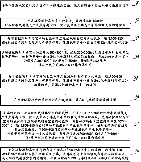
[0028] Such as figure 1 As shown, the passivation method of the semiconductor laser cavity surface provided by the embodiment of the present invention includes the following steps S1 to S8:

[0029] S1, cleave the semiconductor laser epitaxial wafer into bars in the air, put it into the coating fixture and put it into the magnetron sputtering vacuum chamber.

[0030] S2, turn on the hydrogen source in the magnetron sputtering vacuum chamber, and generate hydrogen plasma by sputtering hydrogen gas with 100-150W radio frequency power, and use the hydrogen plasma to...


PUM

PropertyMeasurementUnit
transmittivityaaaaaaaaaa
reflectanceaaaaaaaaaa
transmittivityaaaaaaaaaa

Abstract

The invention provides a passivation method of a semiconductor laser cavity surface and a semiconductor laser, belonging to the field of semiconductor lasers. By bombarding and injecting nitrogen plasma into the front and back cavity surfaces of semiconductor lasers, the hanging bonds on the cavity surface can be fully bonded to N atoms, which can not only passivate N atoms, but also cause the formation of Ga-N bond is more stable; By bombarding and implanting the front and back cavity surfaces with carbon plasma, C atoms are fully combined with the new broken bonds produced by nitrogen ion bombardment, which compensates the surface damage of the cavity surface and ensures the saturation and stability of the hanging bonds of the cleavage cavity surface. Therefore, the invention not only simplifies the process steps of cavity surface passivation, reduces the process flow time, reduces the production cost, but also improves the anti-optical catastrophe level of the semiconductor laser and the reliability of stable output under the condition of high optical power density, and realizes the purpose of high power and long service life of the semiconductor laser.

Description

technical field [0001] The invention relates to the technical field of semiconductor lasers, in particular to a passivation method for a cavity surface of a semiconductor laser and a semiconductor laser. Background technique [0002] Semiconductor lasers have the characteristics of high near-infrared repetition rate and high peak power, and also have the advantages of small size, low energy consumption and long life, so they are widely used in many fields. However, in the process of cleaving the bar and installing the bar coating of the semiconductor laser, because its cleavage surface is a non-polar surface, it is composed of a cation and an anion, that is, the nearest neighbor chemical bonds in the compound semiconductor are heterosexual, and there is no Like a covalent bond that shares electron pairs, it is more like an ionic bond, and the atom that occupies more electrons is negative. Therefore, III-V compounds are cleaved along the cleavage plane, and a small amount of...

Claims


Application Information

Patent Timeline
Patent Type & Authority Patents(China)
IPC IPC(8): H01S5/028H01S5/10
CPCH01S5/0282H01S5/10
Inventor 董海亮米洪龙许并社梁建贾志刚关永莉王琳张乔
Owner SHANXI FEIHONG LASER TECH
Why Eureka
Try Eureka