A method for optimizing the resolving power of electron beam lithography machine

An electron beam exposure machine and a technology with analytical capabilities, which are used in opto-mechanical equipment, microlithography exposure equipment, photolithography process exposure devices, etc. high contrast effect

Inactive Publication Date: 2018-12-25
WUXI ZHONGWEI MASK ELECTRONICS
View PDF3 Cites 0 Cited by
  • Summary
  • Abstract
  • Description
  • Claims
  • Application Information

AI Technical Summary

Problems solved by technology

[0004] In the high-end mask manufacturing of 0.13 micron and above technology nodes, it is particularly important to be able to write the customer's graphics on the mask completely through the exposure equipment, but in fact it is

Method used


Image

  • A method for optimizing the resolving power of electron beam lithography machine
  • A method for optimizing the resolving power of electron beam lithography machine
  • A method for optimizing the resolving power of electron beam lithography machine

Examples


Embodiment Construction

[0022] The preferred embodiments of the present invention will be described below in conjunction with the accompanying drawings. It should be understood that the preferred embodiments described here are only used to illustrate and explain the present invention, and are not used to limit the present invention.

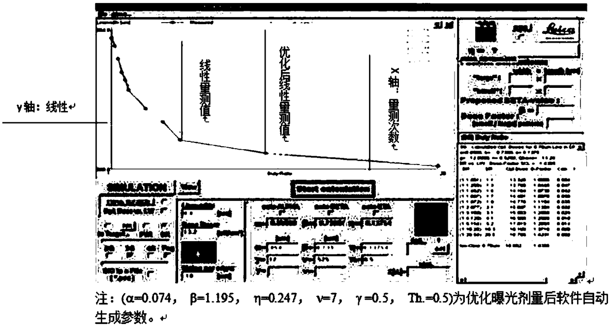
[0023] Exposure equipment: Leica SB350, the support technology node of the exposure equipment is 0.13μm mask production, in the current process,

[0024] There are several aspects to improve the analytical capabilities of the exposure machine:

[0025] (1) The characteristics of electronic resists: resists are also called photosensitive glues. After electron beam exposure of commonly used linear chain high-molecular polymers, the polymer will undergo both chain scission and cross-chain reactions. Any resist with a dominant chain scission reaction is called a positive resist, and any resist with a dominant cross-chain reaction is called a negative resist. At present, the resist...


PUM


Abstract

The invention discloses an optimization method for the resolution ability of an electron beam exposure machine, which comprises the following steps: (1) optimizing the characteristics of an electronicresist: selecting a FEP positive photoresist, wherein the photoresist has high sensitivity, high resolution and contrast; (2) optimization of proximity effect: adopting software correction measures to correct proximity effect by adjusting the geometry of wavefront engineering, or by exposure dose modulation, or by combining the two; (3) Optimization of developing program of developing machine: baking after exposure. The method of the invention finds a critical point of the maximum resolution capability of the current exposure equipment, and at the same time, searches for the possibility of improving the exposure resolution capability of the mask without changing the exposure equipment by optimizing the exposure process, so as to meet the exposure process requirements of the high-end mask.

Description

Technical field [0001] The invention relates to a method for optimizing the analytical capability of an electron beam exposure machine. Background technique [0002] The development of modern microelectronics technology basically follows Moore's Law, that is to say: Every 18 months or so, the feature size of integrated electrical components should be reduced by 1 / 2, and the integration density should be doubled. Western developed countries regard microelectronics technology as a strategic industry and strictly impose technical blockade restrictions on developing countries. Today, INTEL (Intel) has been able to put into production integrated circuits with a component size of about 10nm, while the corresponding level in my country is only 40nm, and the processing level is two generations (ie 20nm, 10nm). At present, the mainstream technology used in the world is optical light. engraved. The light source of optical lithography has developed from long-wavelength infrared rays to tod...

Claims


Application Information

Patent Timeline
IPC IPC(8): G03F7/20
CPCG03F7/2059G03F7/2061G03F7/70441
Inventor 沙云峰刘维维刘浩
Owner WUXI ZHONGWEI MASK ELECTRONICS
Why Eureka
Try Eureka