A high speed memory chip having multiple independent access channels

A memory chip and independent access technology, which is applied in the direction of instruments, electrical digital data processing, etc., can solve the problems of high storage price, difficult interface implementation, high cost ratio, etc., to achieve data sharing and data exchange, total storage Cost reduction, storage and processing effects

Active Publication Date: 2018-12-25
深圳市安信智控科技有限公司
View PDF12 Cites 10 Cited by
  • Summary
  • Abstract
  • Description
  • Claims
  • Application Information

AI Technical Summary

Problems solved by technology

First, the bandwidth improvement of these storage technologies is limited. They use a multi-bit parallel interface bus. The main way to further increase the bandwidth is to use a wider interface bus or increase the interface rate, but the multi-bit parallel bonded transmission requires signal integrity. It is becoming more and more difficult to implement higher, wider and higher-speed interfaces
Second, the implementation cost of new storage technology is relatively high. For example, the engineering cost of advanced HBM technology is as high as tens of millions of dollars.
The third is that the above-mentioned new storage technologies do not have a sharing mode, or the sharing granularity is very low. For example, DDR4 / DDR5, GDDR5, and HBM storage media can only be accessed by the main control chip directly connected to them, and cannot realize multiple storage. Direct shared access of multiple main control chips; although HMC can support the connection of multiple main control chips, it does not support the shared use of more than four main control chips
In addition, limited by the production capacity of storage suppliers, storage is in an unbalanced state of supply and demand, which pushes up the selling price of storage, making the cost of storage in the system more and more high, and the cost of the above-mentioned new types of storage is even higher. It also severely restricts the large-scale application of new storage technologies and memory chip products.

Method used


Image

  • A high speed memory chip having multiple independent access channels
  • A high speed memory chip having multiple independent access channels
  • A high speed memory chip having multiple independent access channels

Examples


Embodiment 1

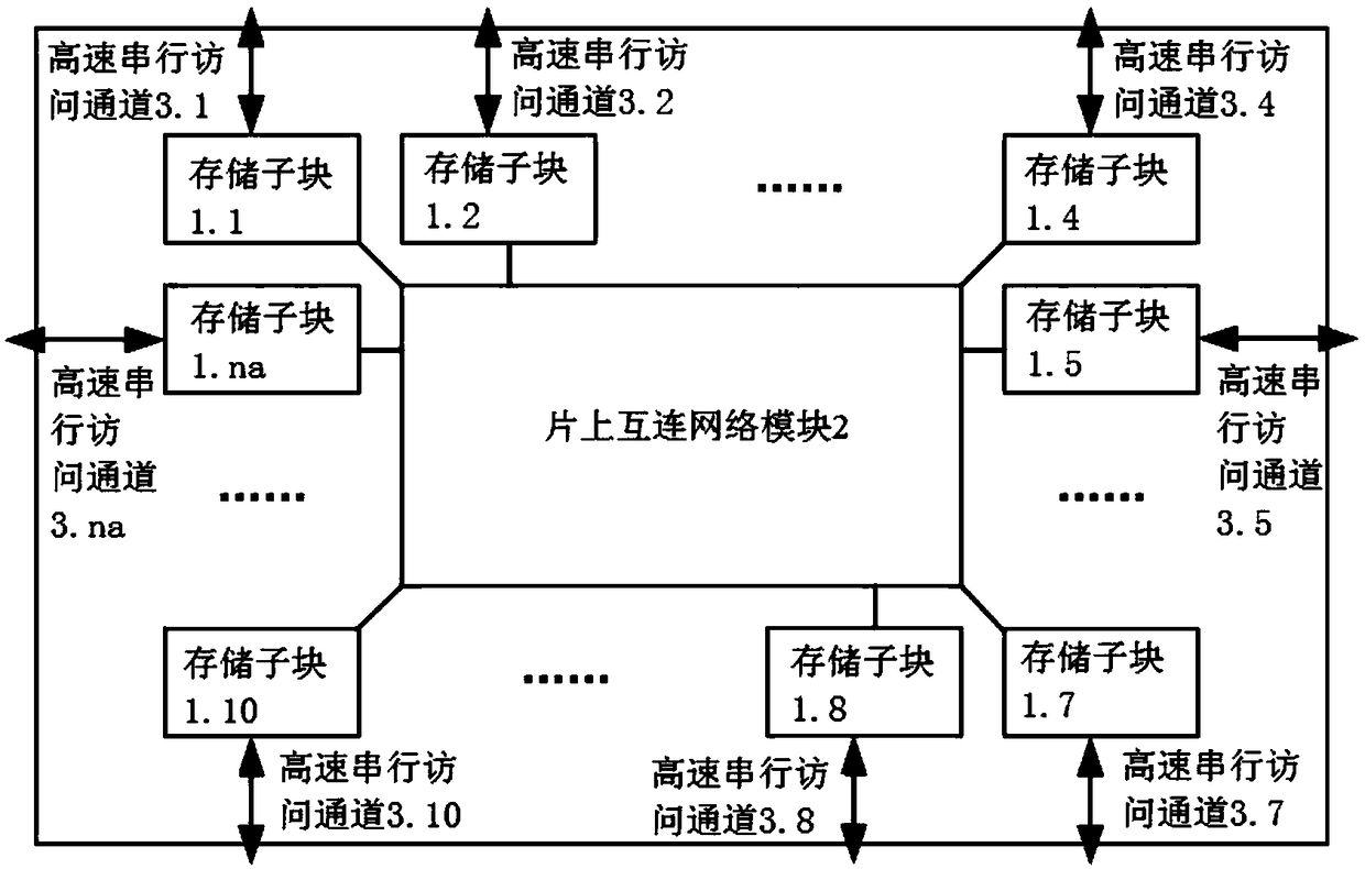
[0035] Such as figure 1 As shown, a high-speed memory chip with multiple independent access channels includes on-chip memory and several high-speed serial access channels. The high-speed serial access channels are respectively marked as 3.1, 3.2, 3.3, ..., 3.na, na is a natural number, and also includes an on-chip interconnection network module 2. The on-chip memory includes several storage sub-blocks that can be accessed in parallel. The storage sub-blocks are respectively marked as 1.1, 1.2, 1.3, ..., 3. The number of row access channels is equal, the high-speed serial access channels are closely coupled with the storage sub-blocks one by one, each high-speed serial access channel is connected with one storage sub-block, and na storage sub-blocks are interconnected through the on-chip interconnection network module 2, Here, the high-speed serial access channel is composed of a single Serdes Lane. From the perspective of the memory chip, the channel receives and sends two dir...

Embodiment 2

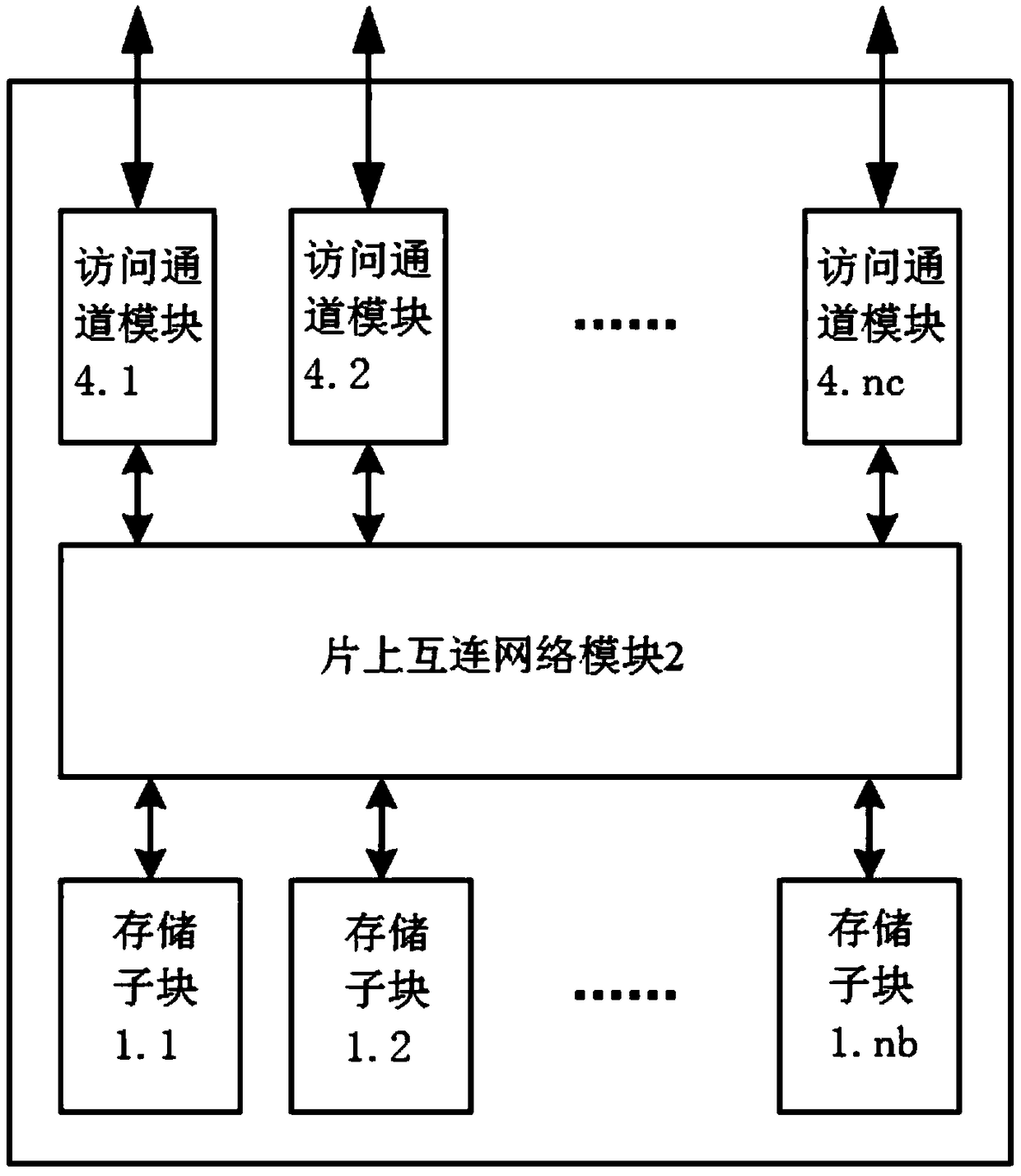
[0039] Such as image 3 As shown, a high-speed memory chip with multiple independent access channels includes an on-chip memory and several high-speed serial access channels, and also includes an on-chip interconnection network module 2. The on-chip memory includes several memory sub-blocks that can be accessed in parallel. The storage sub-blocks are respectively marked as 1.1, 1.2, 1.3, ..., 1.nb, the high-speed serial access channel is loosely coupled with the storage sub-block, the high-speed serial access channel is connected with the on-chip interconnection network module 2 through the access channel module, and access The channel modules are marked as 4.1, 4.2, 4.3, .

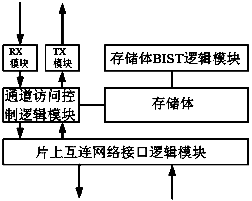
[0040] Such as Figure 4 As shown, the access channel module includes a channel access control logic module. The channel access control logic module communicates with the high-speed serial access channel through the RX module and the TX module respectively. The channel access control logic module is conn...


PUM


Abstract

The invention relates to the field of computer system structure and integrated circuit design, and a high-speed memory chip having a plurality of independent access channels is disclosed, including anon-chip memory and several high-speed serial access channels. A network-on-chip interconnect module is also included. The on-chip memory includes a plurality of memory sub-blocks accessible in parallel, and the memory sub-blocks and the high speed serial access channels are interconnected by the on-chip interconnect network module, and the on-chip interconnect network module being implemented ina single bus, a multi-bus, a ring network, a two-dimensional mesh, or a crossbar switch. The invention has a high-speed memory chip with a plurality of independent access channels, has good bandwidthexpansibility, realizes the shared parallel access of a plurality of main control chips to the memory chip and the data sharing and exchange among the plurality of main control chips, integrates storage and processing, and reduces the total storage cost of the system and the design and manufacture cost of the memory chip.

Description

technical field [0001] The invention relates to the field of computer system structure and integrated circuit design, in particular to a high-speed memory chip with multiple independent access channels. Background technique [0002] In a computer system, the storage subsystem plays a very important role and plays a very important role in the overall performance of the system, especially for those memory-intensive algorithms, the memory access bandwidth and delay are the key factors that determine the performance of the algorithm. Judging from the status quo of technological development, the improvement of storage performance lags far behind the improvement of computing performance. [0003] The industry develops new storage technologies from a variety of different technical approaches, such as DDR4 / DDR5, GDDR5, HMC (Hybrid Memory Cube), HBM (High Bandwidth Memory), etc. Although various new storage technologies can improve memory access bandwidth higher and higher, there ar...

Claims


Application Information

Patent Timeline
Patent Type & Authority Applications(China)
IPC IPC(8): G06F13/16G06F13/378
CPCG06F13/1663G06F13/378
Inventor 童元满陆洪毅刘垚童乔凌
Owner 深圳市安信智控科技有限公司
Why Eureka
Try Eureka