Display backplane, preparation method thereof, and display device

A display backplane, transparent technology, applied in semiconductor/solid-state device manufacturing, electrical components, electrical solid-state devices, etc., can solve the problem of separating the characteristics of driving thin film transistors and switching thin film transistors

Active Publication Date: 2019-01-04
BOE TECH GRP CO LTD +1
View PDF7 Cites 11 Cited by
  • Summary
  • Abstract
  • Description
  • Claims
  • Application Information

AI Technical Summary

Problems solved by technology

[0004] The technical problem to be solved by the embodiments of the present invention is to provide a display backplane, its preparation method, and a display device, so as

Method used


Image

  • Display backplane, preparation method thereof, and display device
  • Display backplane, preparation method thereof, and display device
  • Display backplane, preparation method thereof, and display device

Examples


no. 1 example

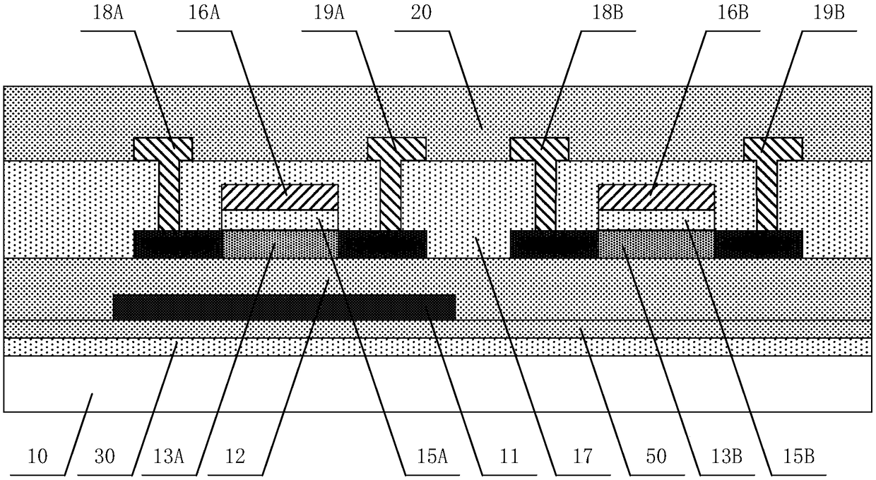
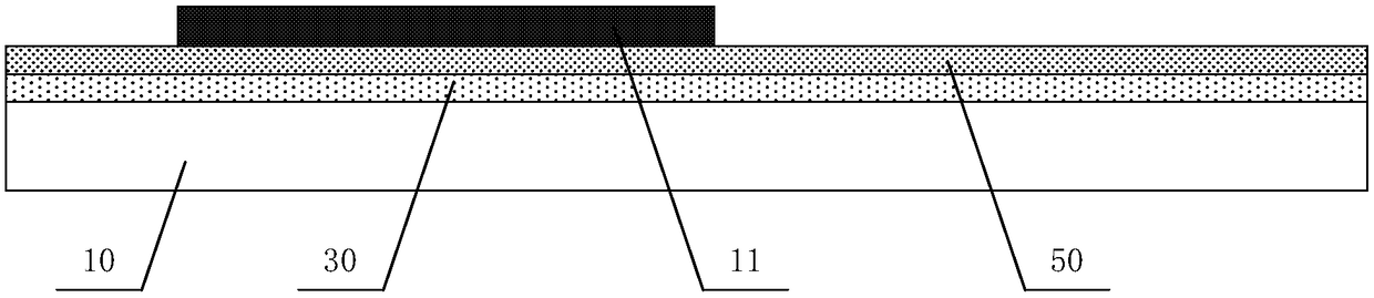
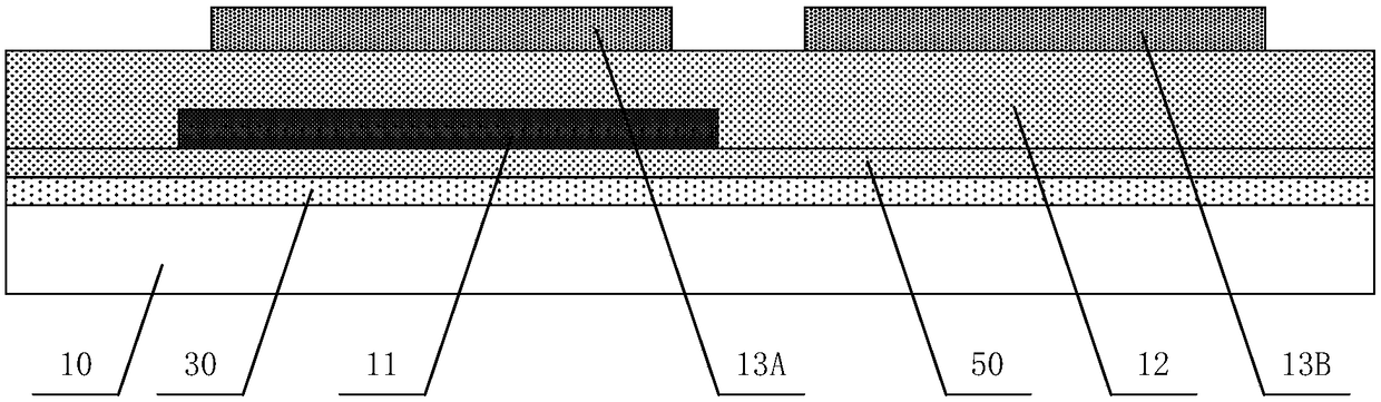
[0066] figure 1 It is a schematic structural diagram of the first embodiment of the display backplane according to the present invention, only illustrating the driving thin film transistor and the switching thin film transistor. Such as figure 1 As shown, the main structure of the top gate bottom emission structure OLED display backplane in this embodiment includes a transparent heat conduction layer formed on the substrate, a shielding layer formed on the transparent heat conduction layer, a top gate type first thin film transistor and a second thin film transistor. The transparent thermal conduction layer includes a transparent conductive layer and a first buffer layer, the first thin film transistor is used as a driving thin film transistor (DRTFT), and the second thin film transistor is used as a switching thin film transistor (SW TFT). Specifically, the present embodiment shows that the backplane includes: a transparent conductive layer 30 and a first buffer layer 50 se...

no. 2 example

[0079] Figure 8 A schematic structural diagram of the second embodiment of the backplane is shown in the present invention. This embodiment is an extension of the aforementioned first embodiment. The main structure of the top-gate bottom-emission structure OLED display backplane includes a transparent heat conduction layer formed on the substrate, a shielding layer formed on the transparent heat conduction layer, and a top-gate type first a thin film transistor and a second thin film transistor. Different from the aforementioned first embodiment, the transparent heat conduction layer of this embodiment includes a transparent semiconductor layer 40 and a first buffer layer 50, such as Figure 8 shown.

[0080] In this embodiment, the material of the transparent semiconductor layer can be metal oxide or silicon material, and the metal oxide can include a metal oxide semiconductor formed by one or more metal elements such as indium (In) or gallium (Ga), such as Indium Gallium...

no. 3 example

[0083] Figure 9 A schematic structural diagram of the third embodiment of the backplane is shown for the present invention. This embodiment is an extension of the aforementioned first and second embodiments. The main structure of the top-gate bottom-emitting structure OLED display backplane includes a transparent heat conduction layer formed on the substrate, a shielding layer formed on the transparent heat conduction layer, and a top-gate type. The first thin film transistor and the second thin film transistor. Different from the aforementioned first and second embodiments, the transparent heat conduction layer in this embodiment includes a transparent conductive layer 30, a transparent semiconductor layer 40 and a first buffer layer 50, such as Figure 9 shown.

[0084] In this embodiment, the material of the transparent conductive layer can be indium tin oxide ITO or indium zinc oxide IZO, the material of the transparent semiconductor layer can be metal oxide or silicon ...


PUM


Abstract

An embodiment of the present invention provides a display backplane, a preparation method thereof, and a display device. The display backplane includes a substrate, a transparent heat conduction layerdisposed on the substrate, and an array structure layer disposed on the heat conduction layer. The array structure layer includes a light shielding layer, a first thin film transistor and a second thin film transistor, and the light shielding layer is disposed between the transparent heat conduction layer and the first thin film transistor. The transparent heat conductive layer comprises a transparent conductive layer, a transparent semiconductor layer or a transparent conductive layer and a transparent semiconductor layer. As that transparent heat conduction lay is arranged between the substrate and the array structure lay, the invention can effectively solve the problem that the characteristics of the driving thin film transistor and the switching thin film transistor of the prior OLEDdisplay device are separated.

Description

technical field [0001] The invention relates to the field of display technology, in particular to a display backplane, a preparation method thereof, and a display device. Background technique [0002] Thin Film Transistor (TFT) is a very important element in the field of display technology, and plays a very important role in Liquid Crystal Display (LCD) and Organic Light Emitting Diode (OLED). At present, there are two main types of thin film transistors: bottom gate thin film transistors and top gate thin film transistors. Since there is no overlapping area between the gate electrode and the source-drain electrode in the top-gate thin film transistor, it has a small parasitic capacitance, and the small parasitic capacitance reduces the delay of the RC circuit, so it has a higher switching speed and is easy Enable higher resolution displays. At the same time, the number of patterning processes required to prepare the top-gate thin film transistor is small, and has the adva...

Claims


Application Information

Patent Timeline
IPC IPC(8): H01L27/12H01L21/77H01L23/367H01L27/32
CPCH01L27/1214H01L27/1259H01L23/367H10K59/12H01L27/1218H01L29/78633H01L27/1262H10K59/126H10K59/1213H10K50/87H10K50/84H10K50/805
Inventor 苏同上王东方王庆贺赵策周斌闫梁臣
Owner BOE TECH GRP CO LTD
Why Eureka
Try Eureka