Substrate for power modules

A power module and substrate technology, which is applied in the direction of circuit substrate materials, improvement of metal adhesion of insulating substrates, welding equipment, etc., can solve problems such as partial discharge characteristics and deterioration of withstand voltage characteristics, and achieve suppression of partial discharge characteristics and withstand voltage characteristics The effect of deterioration, suppression of partial discharge, and suppression of charge concentration

Active Publication Date: 2019-01-04
MITSUBISHI MATERIALS CORP
View PDF8 Cites 0 Cited by
  • Summary
  • Abstract
  • Description
  • Claims
  • Application Information

AI Technical Summary

Problems solved by technology

Among them, depending on the shape of the remaining Cu-Sn layer and intermetallic compound layer, charges may be locally concentrated at the end of the circuit pattern of the circuit layer, resulting in deterioration of partial discharge characteristics and withstand voltage characteristics.

Method used


Image

  • Substrate for power modules
  • Substrate for power modules
  • Substrate for power modules

Examples


Embodiment

[0103]

[0104] Hereinafter, the results of confirmation experiments conducted to confirm the effects of the present invention will be described.

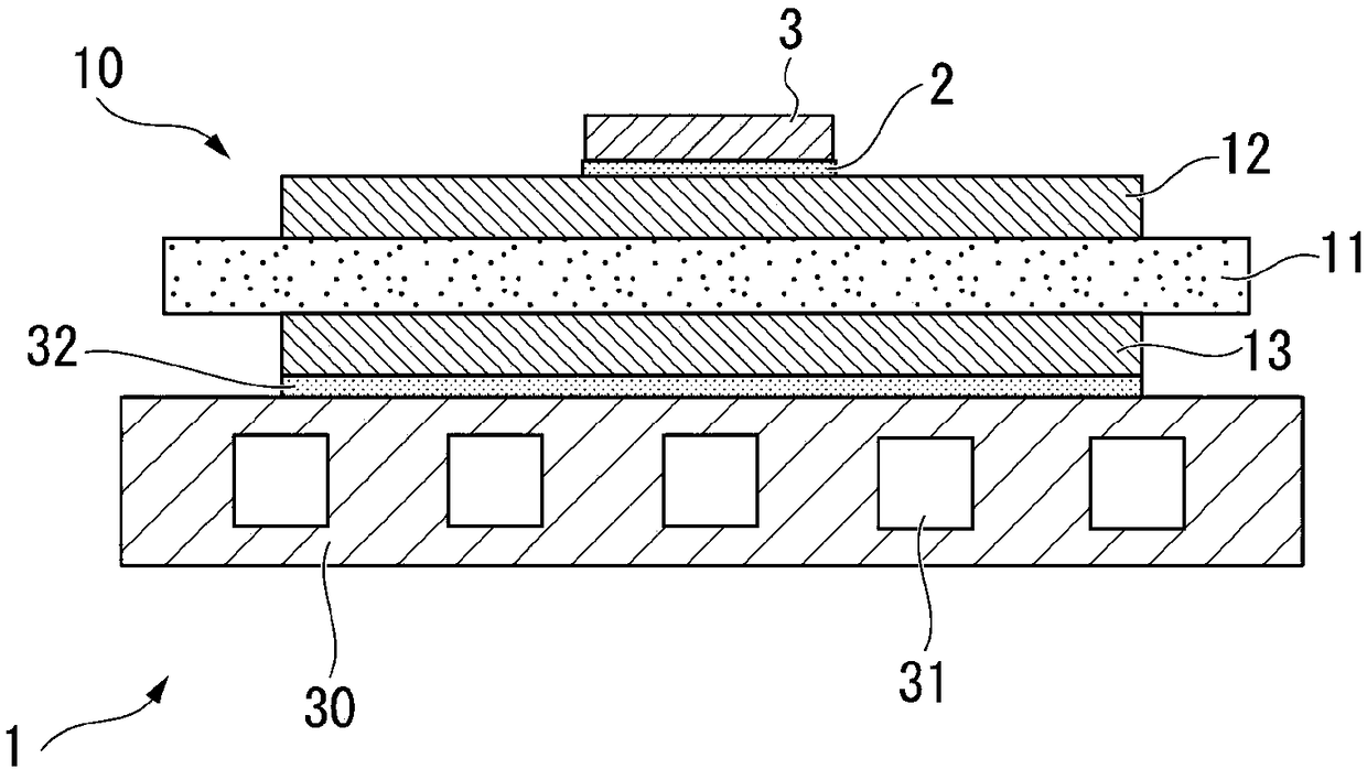
[0105] According to the procedures described in the above-mentioned embodiments, the ceramic substrates shown in Table 1 and Table 2 (50mm×60mm×thickness 0.635mm (AlN), 50mm×60mm×thickness 0.32mm (Si 3 N 4 ))) were bonded to one surface and the other surface of Cu plates (46 mm x 56 mm x thickness 0.3 mm) shown in Table 1 and Table 2 to form a circuit layer and a metal layer. As the Cu plate, oxygen-free copper ("OFC" in Table 1 and Table 2) or tough copper ("tough copper" in Table 1 and Table 2) was used. Cu-P-Sn based solder with a thickness of 25 μm was used.

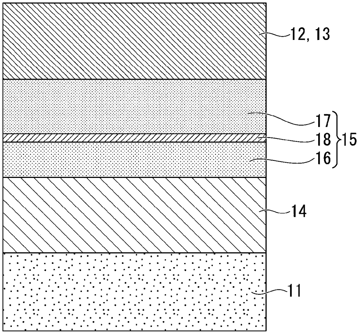
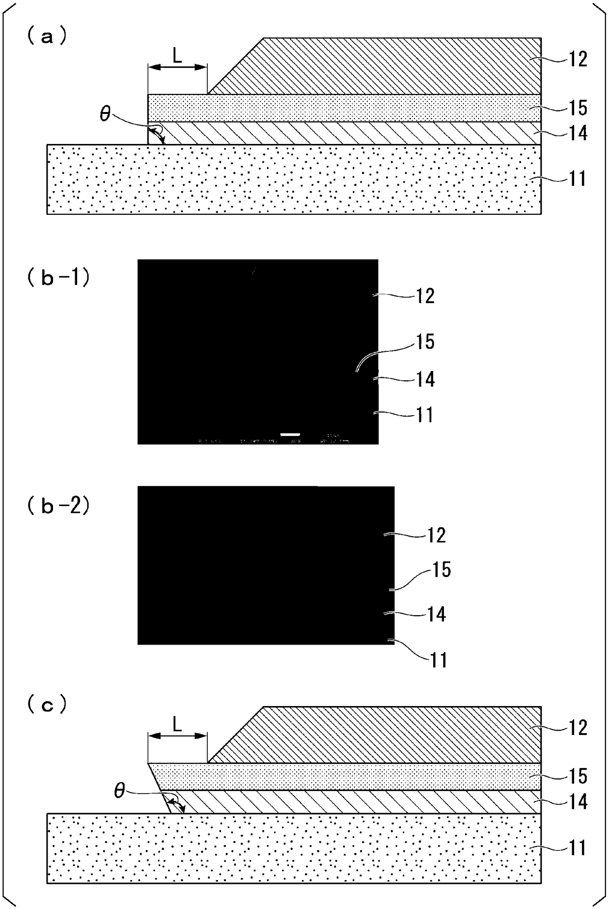
[0106] Then, the etching process described in the above-mentioned embodiment was performed on the circuit layer, thereby forming a circuit pattern with a distance between wirings of 500 μm. Specifically, in Cu etching process S31, spray etching was performed for 5 to...


PUM

PropertyMeasurementUnit
thicknessaaaaaaaaaa
thicknessaaaaaaaaaa
thicknessaaaaaaaaaa

Abstract

This substrate for power modules is provided with a ceramic substrate and a circuit layer having a circuit pattern. At the interface between the circuit layer and the ceramic substrate, a Cu-Sn layerand a Ti-containing layer are sequentially laminated from the ceramic substrate side. With respect to the cross-sectional shape of an end portion of the circuit pattern of the circuit layer, the angletheta between the surface of the ceramic substrate and the end face of the Cu-Sn layer is within the range of from 80 degrees to 100 degrees (inclusive), and the maximum projection length L of the Cu-Sn layer or the Ti-containing layer from the end face of the circuit layer is within the range of from 2 [mu]m to 15 [mu]m (inclusive).

Description

technical field [0001] The present invention relates to a substrate for a power module including a ceramic substrate and a circuit layer having a circuit pattern formed on one surface of the ceramic substrate. [0002] This application claims priority based on Patent Application No. 2016-100615 for which it applied in Japan on May 19, 2016, and uses the content here. Background technique [0003] A semiconductor device such as an LED or a power module has a structure in which a semiconductor element is bonded to a circuit layer made of a conductive material. [0004] Power semiconductor elements for high-power control used to control electric vehicles such as wind power generation and electric vehicles generate a large amount of heat. Therefore, substrates for mounting such elements have been widely used. For example, AlN (aluminum nitride) A substrate for power modules in which a metal plate with excellent electrical conductivity is bonded to one surface of a ceramic subst...

Claims


Application Information

Patent Timeline
Patent Type & Authority Applications(China)
IPC IPC(8): H01L23/13H01L23/12H01L23/36H05K1/03H05K3/38
CPCH01L2224/32225B23K35/22H01L23/3735H01L23/3731C04B37/026C04B2237/124C04B2237/122C04B2237/366C04B2237/368C04B2237/407H01L23/13H05K3/38H05K1/03H01L23/36H01L23/12H01L23/49822H05K1/0298H05K1/0306
Inventor 大桥东洋长友义幸
Owner MITSUBISHI MATERIALS CORP
Why Eureka
Try Eureka