

Growth process method of large-diameter high-purity semi-insulating silicon carbide
A process method and semi-insulating technology, which are applied in the field of large-diameter high-purity semi-insulating silicon carbide growth, can solve the problems affecting the yield and technical indicators of the substrate, and the low utilization rate of raw materials, so as to achieve a low nitrogen content and improve the utilization rate. Effect
- Summary
- Abstract
- Description
- Claims
- Application Information
AI Technical Summary
Problems solved by technology
Method used
Image

Examples
Embodiment 1
[0058] Embodiment 1. Large-diameter high-purity semi-insulating silicon carbide growth process
[0059] Using the thermal field of the dual heating structure and the bottom diffusion structure of the present application, the PVT method is used to grow a high-purity semi-insulating silicon carbide single crystal, and the specific steps are as follows:
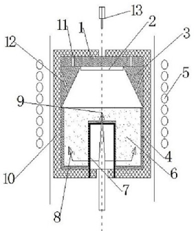
[0060] 1. Place the high-purity silicon carbide raw material in the graphite crucible, and the upper part of the crucible is assembled as follows figure 1 The structure of seed holder, 2 seeds, and 3 expansion rings. The exterior is wound with a thermal insulation layer according to the process design. Material selection graphite carbon fiber. The above assembly is called the growth thermal field, and all the graphite materials are high-purity graphite materials, and the purity requirement is <5ppm purified graphite.
[0061] 2. Place the assembly growth heat field completed in step 1 in a single crystal growth furnace, and e...
Embodiment 2
[0070] Embodiment 2. Large-diameter high-purity semi-insulating silicon carbide growth process
[0071] Using the thermal field of the dual heating structure and the bottom diffusion structure of the present application, the PVT method is used to grow a high-purity semi-insulating silicon carbide single crystal, and the specific steps are as follows:
[0072] 1. Place the high-purity silicon carbide raw material in the graphite crucible, and the upper part of the crucible is assembled as follows figure 1 The structure of seed holder, 2 seeds, and 3 expansion rings. The exterior is wound with a thermal insulation layer according to the process design. Material selection graphite carbon fiber. The above assembly is called the growth thermal field, and all the graphite materials are high-purity graphite materials, and the purity requirement is <5ppm purified graphite.
[0073] 2. Place the assembly growth heat field completed in step 1 in a single crystal growth furnace, and e...
Embodiment 3
[0082] Embodiment 3. Large-diameter high-purity semi-insulating silicon carbide growth process
[0083] Using the thermal field of the dual heating structure and the bottom diffusion structure of the present application, the PVT method is used to grow a high-purity semi-insulating silicon carbide single crystal, and the specific steps are as follows:
[0084] 1. Place the high-purity silicon carbide raw material in the graphite crucible, and the upper part of the crucible is assembled as follows figure 1 The structure of seed holder, 2 seeds, and 3 expansion rings. The exterior is wound with a thermal insulation layer according to the process design. Material selection graphite carbon fiber. The above assembly is called the growth thermal field, and all the graphite materials are high-purity graphite materials, and the purity requirement is <5ppm purified graphite.
[0085] 2. Place the assembly growth heat field completed in step 1 in a single crystal growth furnace, and e...
PUM
| Property | Measurement | Unit |
|---|---|---|
| porosity | aaaaa | aaaaa |
Abstract
Description
Claims
Application Information