Solder for flip chip LED and application thereof
A solder and flip-chip technology, applied in the direction of welding/cutting media/materials, welding media, welding equipment, etc., can solve the problems of poor heat dissipation and reliability, reduce soldering void rate, and low production efficiency, so as to improve stability and Reliability, improved heat dissipation performance, and improved productivity
- Summary
- Abstract
- Description
- Claims
- Application Information
AI Technical Summary
Problems solved by technology
Method used
Image

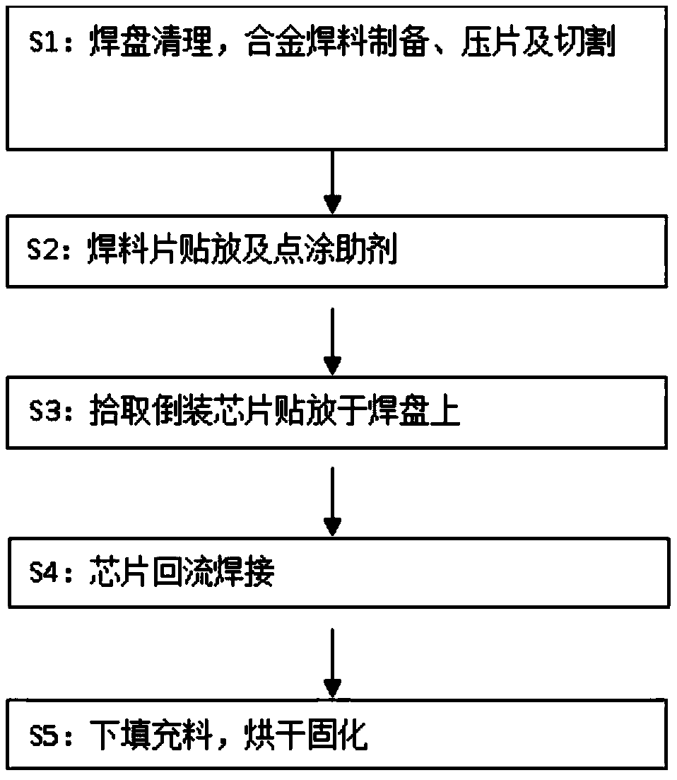
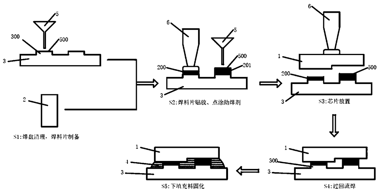
Examples
Embodiment 1
[0046] Embodiment 1 A kind of solder for flip-chip LED
[0047] A kind of solder used for flip-chip LED chips is a Sn-Zn-Cu alloy material, wherein, in terms of mass percentage, the content of Sn is 80%, the content of Zn is 18.5%, and the content of Cu is 1.5%.
[0048] The melting point of the solder ranges from 220°C to 300°C, the thermal conductivity is greater than 70W / (m·K), and the hardness is 16HV, which can effectively absorb the thermal stress generated by the heating of the substrate and chip.
Embodiment 2
[0049] Embodiment 2 Preparation of a kind of solder for flip-chip LED
[0050]The preparation of the solder uses a vacuum high-frequency induction melting furnace for secondary melting, and argon is filled as a protective gas during the melting process to prevent metal oxidation. The metal is melted at high temperature for the first time, and mechanically stirred at medium temperature for the second time to homogenize the components of the alloy.
[0051] After the preparation is completed, the alloy solder is cast into blocks, and pressed into tablets by a tablet press.
[0052] For different pad 300 shapes, utilize laser or mold to cut out required thin solder sheet 200, thick solder sheet 201, complete the preparation of solder sheet 2.
Embodiment 3
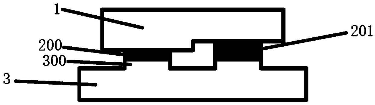
[0053] Embodiment 3 A flip-chip LED (single chip)
[0054] A flip-chip LED chip, such as image 3 , Figure 4 , consisting of a substrate, pad, solder layer, and chip from bottom to top; and fill the gap between the substrate and the chip, and around the solder layer with insulating heat-conducting glue.
[0055] Wherein, the pads can be copper pads, aluminum pads, etc.; there is no solder bump or electroplated solder layer on the pads.
[0056] Wherein, the chip adopts GaAs, sapphire or silicon substrate material.
[0057] Wherein, the main component of the insulating and thermally conductive adhesive is selected from one or more of epoxy resin, acrylic resin, and silicone resin.
PUM
| Property | Measurement | Unit |
|---|---|---|
| melting point | aaaaa | aaaaa |
| hardness | aaaaa | aaaaa |
| thickness | aaaaa | aaaaa |
Abstract
Description
Claims
Application Information
 - R&D
- Intellectual Property
- Life Sciences
- Materials
- Tech Scout
- Unparalleled Data Quality
- Higher Quality Content
- 60% Fewer Hallucinations
Browse by: Latest US Patents, China's latest patents, Technical Efficacy Thesaurus, Application Domain, Technology Topic, Popular Technical Reports.
© 2025 PatSnap. All rights reserved.Legal|Privacy policy|Modern Slavery Act Transparency Statement|Sitemap|About US| Contact US: help@patsnap.com