ion implanter

An ion implanter and ion source technology, applied in circuits, discharge tubes, electrical components, etc., can solve problems such as metal pollution and affect the performance of semiconductor devices, prevent metal ions, reduce the generation of metal ions, and improve yields Effect

Active Publication Date: 2020-12-08
淮安西德工业设计有限公司
View PDF6 Cites 0 Cited by
  • Summary
  • Abstract
  • Description
  • Claims
  • Application Information

AI Technical Summary

Problems solved by technology

These metal ions will be mixed in the ion beam, causing metal contamination and affecting the performance of semiconductor devices

Method used


Image

  • ion implanter
  • ion implanter
  • ion implanter

Examples


Embodiment approach 1

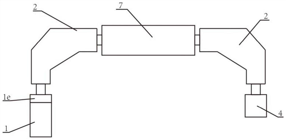
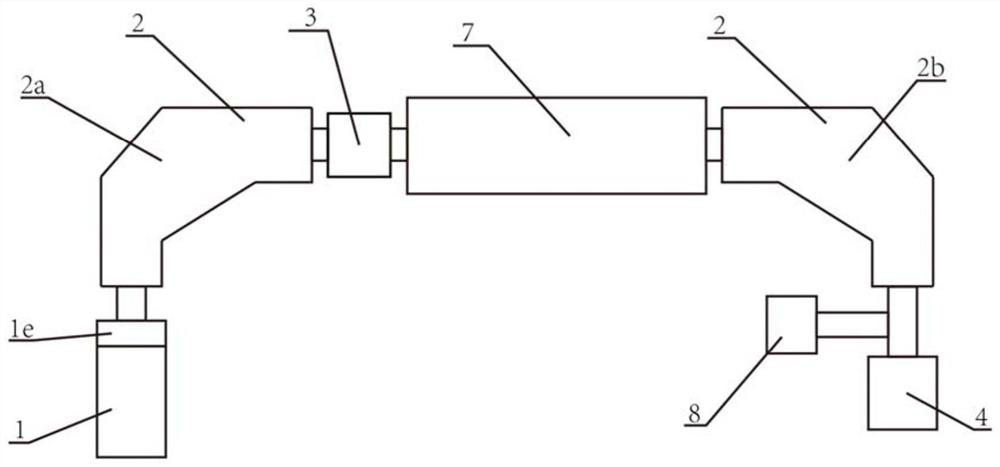
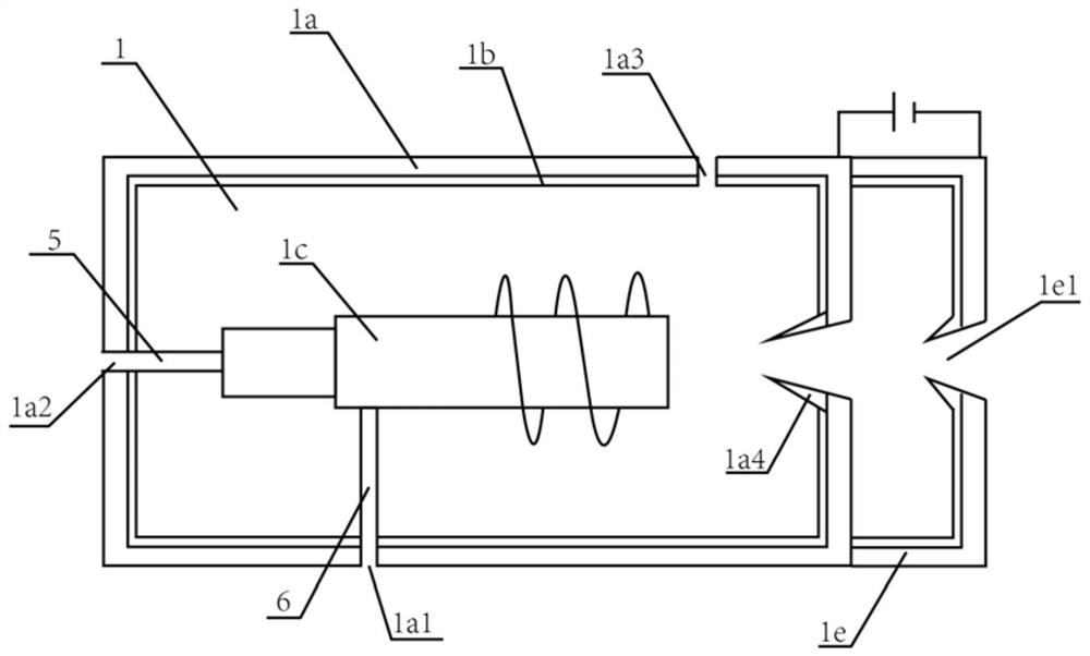
[0055] This embodiment provides an ion implanter, see figure 2 and image 3 As shown, it includes: ion source structure 1, analysis magnet 2, valence state conversion device 3 and process chamber 4; wherein, ion source structure 1 generates plasma through inductively coupled plasma technology and forms an ion beam; analysis magnet 2 is located in the ion The downstream of the source structure 1 is used to deflect the ion beam and select the ions in it to form an implanted ion beam; the valence conversion device 3 is connected to the analysis magnet 2, and can analyze the implanted ions after the analysis magnet 2 The valence state of the ions in the beam is converted; the process chamber 4 is arranged downstream of the valence state conversion device 3, and the wafer is placed in the process chamber 4, and the process chamber 4 is the place where the implanted ion beam bombards the wafer.

[0056] The ion implanter provided in this embodiment applies inductively coupled plas...

Embodiment approach 2

[0085] During the implantation process, the implanted ion beam bombards the wafer, causing positive ions to accumulate on the wafer, forming a large amount of charge on the wafer surface, changing the charge balance in the implanted ion beam, thereby affecting the dose of ion implantation . And because the surface of the wafer is usually formed with different patterns, the charged ions continuously scan the wafer during the ion implantation process, which may cause tip discharge on the wafer surface, thereby affecting the quality of ion implantation.

[0086] To solve this problem, a common method is to spray the wafer with electrons, that is, to spray low-energy electrons to the surface of the wafer. Specifically, before the implant ion beam is scanned onto the wafer surface, low-energy electrons are incorporated into the implant ion beam, thereby neutralizing the positive charge on the wafer surface and improving the effect of ion implantation.

[0087] In the prior art, th...

Embodiment approach 3

[0096] The third embodiment of the present invention provides an ion implantation method, see Figure 6-Figure 8 As shown, the ion implantation method according to the third embodiment of the present invention includes: an ion generation step, supplying energy to gas molecules and ionizing them, generating plasma by inductively coupled plasma technology and forming an ion beam; an ion selection step, ionizing The ion species in the beam is selected, the required ions are separated, and the implanted ion beam is formed; there is also a valence conversion step between the ion selection step and the ion acceleration step, and the implanted ion beam is bombarded by charged particles to make the implanted ion beam The valence state of the ions in the ion beam changes; the ion acceleration step, by applying a voltage to the implanted ion beam, adjusts the energy of the implanted ion beam; the ion implantation step, the implanted ion beam bombards the surface of the wafer, thereby per...


PUM


Abstract

The invention relates to the technical field of semiconductor equipment manufacturing, and discloses an ion implanting machine and an ion implanting method. The ion implanting machine comprises an ionsource structure, wherein the ion source adopted by the ion source structure is an inductively coupled plasma source. The analysis magnet is connected with the ion source structure, and can receive the implanted ion beam provided by the ion source structure and separate to obtain the implanted ion beam. The valence state conversion device is connected to the analysis magnet and is capable of receiving an implanted ion beam emitted from the analysis magnet and converting the valence state of ions in the implanted ion beam. The ion source structure of the ion implanter of the present inventionforms a plasma to be implanted by inductively coupled plasma technology. Since the metal device is not required to participate in the whole working process of the ion source structure, the generationof metal ions is reduced from the source. Moreover, the valence state of ions implanted in ion beam can be converted by the valence state conversion device, so as to improve the applicability of ion implantation machine.

Description

technical field [0001] The invention relates to the technical field of semiconductor equipment manufacturing, in particular to an ion implanter and an ion implantation method. Background technique [0002] At present, ion implanters are widely used in the production and manufacture of semiconductor devices. By doping a small amount of impurities in the wafer, the structure and conductivity of the wafer can be changed. The impurities usually doped are elements of group IIIA and group VA. . The ion implanter generates plasma of a specific valence state through the ion source structure, and forms an ion beam, which is selected and accelerated and finally bombarded on the wafer, thereby realizing the implantation of specific ions. [0003] However, in the process of generating plasma in the ion source structure, other ions may be introduced, and common impurity ions are metal ions. These metal ions will be mixed in the ion beam, thereby causing metal contamination and affectin...

Claims


Application Information

Patent Timeline
Patent Type & Authority Patents(China)
IPC IPC(8): H01J37/32
CPCH01J37/321H01J37/32422H01J37/3244
Inventor 田成俊洪纪伦吴宗祐林宗贤
Owner 淮安西德工业设计有限公司
Why Eureka
Try Eureka