
Charge pump circuit with low miss ratio for delay phase-locked loop

A delay-locked loop and charge pump technology, applied in the field of microelectronics, can solve the problem of large charge/discharge current mismatch rate and other problems

Active Publication Date: 2019-01-11
CHONGQING UNIV OF POSTS & TELECOMM
View PDF4 Cites 8 Cited by
  • Summary
  • Abstract
  • Description
  • Claims
  • Application Information

AI Technical Summary

Problems solved by technology

However, the charge pump circuit with this structure has effects such as charge injection and clock feedthrough, and the charge / discharge current mismatch rate of the charge pump circuit is relatively large.

Method used


Image

  • Charge pump circuit with low miss ratio for delay phase-locked loop
  • Charge pump circuit with low miss ratio for delay phase-locked loop
  • Charge pump circuit with low miss ratio for delay phase-locked loop

Examples


Embodiment

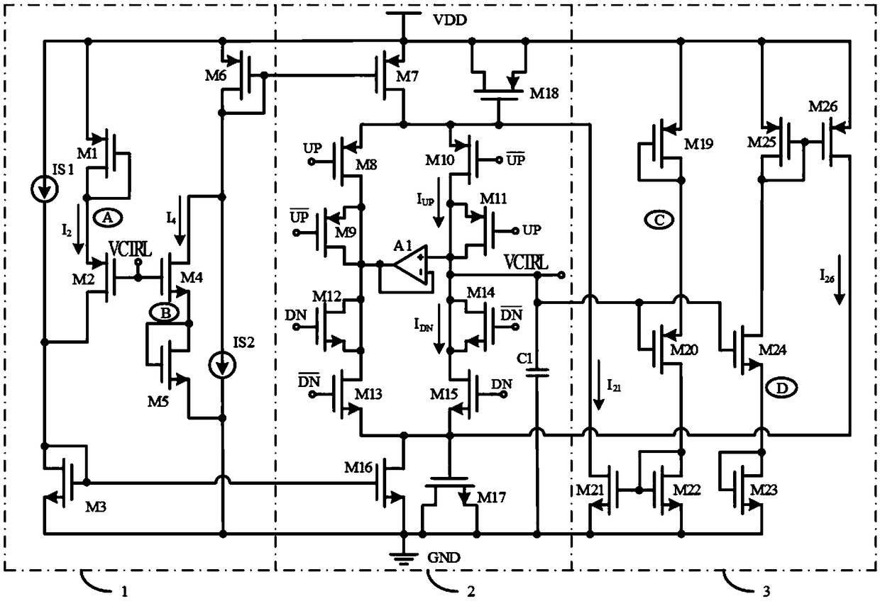
[0030] A low-mismatch charge pump circuit for delay-locked loops, such as figure 2 As shown, it includes a bias circuit 1 with current compensation, a current wheel charge pump circuit 2 and a negative feedback current compensation circuit 3;

[0031] Wherein, the signal output terminal of the bias circuit 1 with current compensation is connected to the signal input terminal of the current wheel charge pump circuit 2, and the signal output terminal VCTRL of the current wheel charge pump circuit 2 is respectively connected to the current The signal input terminal of the compensated bias circuit 1 and the negative feedback current compensation circuit 3 , the signal output terminal of the negative feedback current compensation circuit 3 is connected to the signal input terminal of the current wheel charge pump circuit 2 .

[0032] The bias circuit 1 with current compensation provides a bias current with compensation characteristics for the current wheel charge pump circuit 2, a...


PUM


Abstract

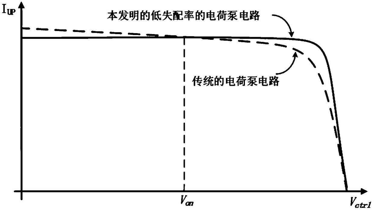
The present invention provides a charge pump circuit with low miss ratio for a delay phase-locked loop. The charge pump circuit mainly comprises a biasing circuit with current compensation, a currentwheeled charge pump circuit and a negative feedback current compensation circuit. The current wheeled charge pump circuit employs a virtual switch tube to effectively inhibit charge injection and clock feedthrough effects, MOS capacitors formed by PMOS tubes M18 and MOS capacitors formed by NMOS tubes M6 are respectively added to source and drain ends of a PMOS tube M7 and source and drain ends ofan NMOS tube M16 to reduce the current glitch when the switch tube of the charge pump circuit opens or closes at the same time; and a compensating current I2, a compensating current I4, a compensating current I21 and a compensating current I26 are led into the current wheeled charge pump circuit to reduce the miss ratio of the charge / discharge current of the charge pump circuit so as to achieve acharge pump circuit with low miss ratio for a delay phase-locked loop.

Description

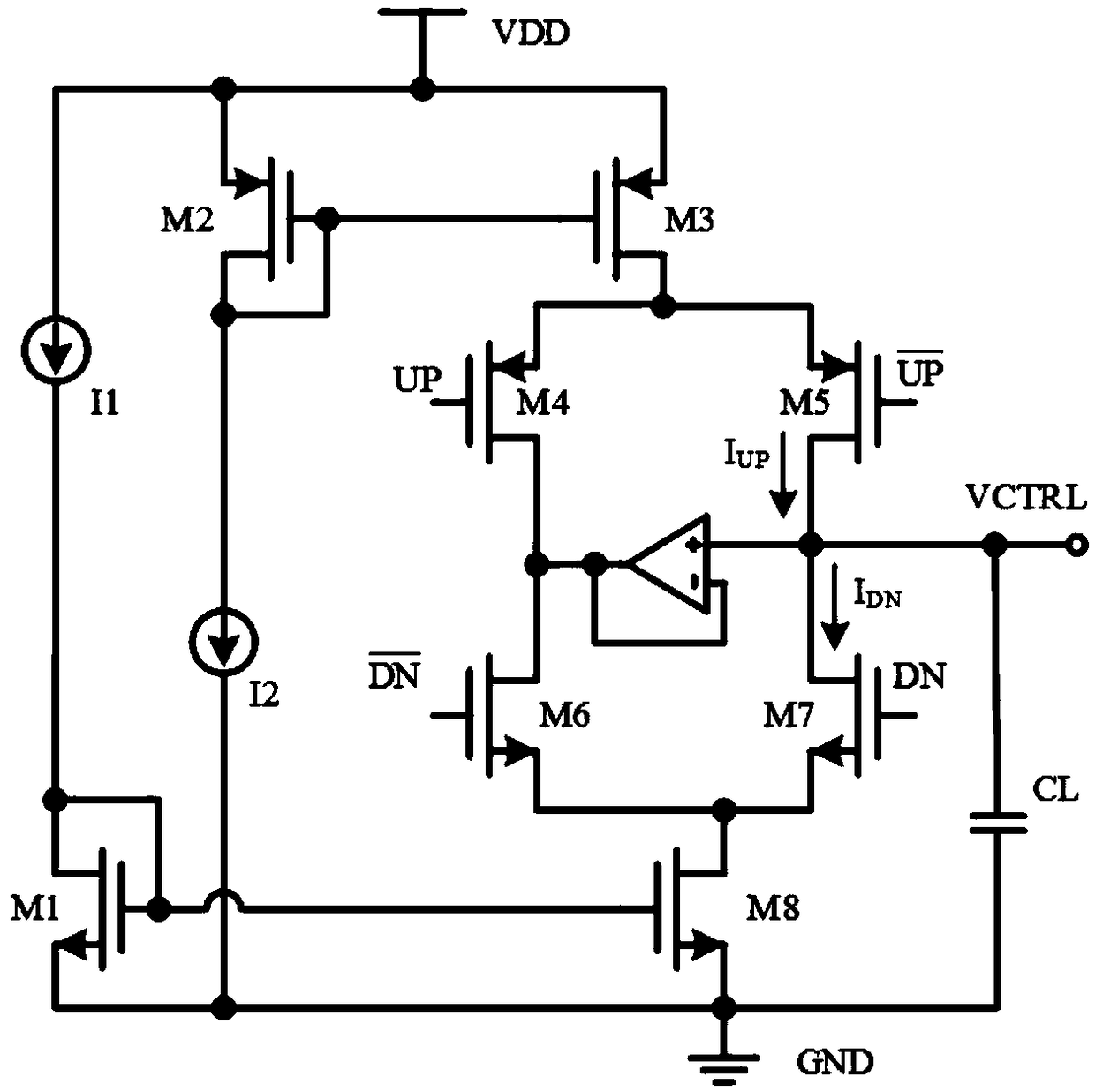
technical field [0001] The invention belongs to the technical field of microelectronics, and in particular relates to a charge pump circuit with low mismatch rate for a delay phase-locked loop. Background technique [0002] The charge pump circuit is one of the main circuit modules of the delay-locked loop, and its performance characteristics directly affect the overall performance characteristics of the delay-locked loop; the main function of the charge pump circuit is to convert the digital pulse signal of the frequency detector into an analog signal. Controls the delay time of the voltage-controlled delay line in the delay-locked loop. [0003] figure 1 It is a traditional charge pump circuit, in which the current source I1 provides bias current for the charge pump circuit through the current mirror composed of NMOS transistor M1 and NMOS transistor M8, and the current source I2 passes through the current mirror composed of PMOS transistor M2 and PMOS transistor M3. The...

Claims


Application Information

Patent Timeline
IPC IPC(8): H03L7/089
CPCH03L7/0891
Inventor 周前能彭志强李红娟关晶晶王永泽
Owner CHONGQING UNIV OF POSTS & TELECOMM
Learn More