
PCB board and IGBT module crimping structure and crimping method

A PCB board and connection structure technology, which is applied in the field of microelectronics, can solve problems such as poor error-proofing ability and increased contact point impedance, and achieve the effects of convenient maintenance, avoiding heat concentration, and improving production efficiency

Active Publication Date: 2019-01-15
HEFEI JUYI POWER SYST CO LTD
View PDF3 Cites 2 Cited by
  • Summary
  • Abstract
  • Description
  • Claims
  • Application Information

AI Technical Summary

Problems solved by technology

Contamination between separable connected parts and oxidation of the surface of the parts can cause sintering effects and lead to increased contact resistance due to contamination or over time
In addition, when the IGBT module and the PCB are screwed and fixed, the screw fixing sequence is strictly required, and the error prevention ability is poor.

Method used


Image

  • PCB board and IGBT module crimping structure and crimping method
  • PCB board and IGBT module crimping structure and crimping method
  • PCB board and IGBT module crimping structure and crimping method

Examples


Embodiment 1

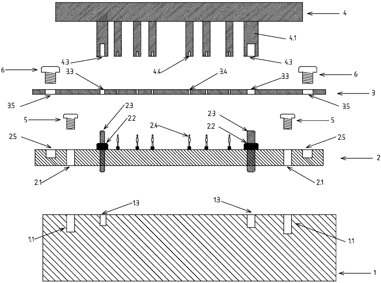
[0047] Such as figure 1An exploded view of the crimping structure between the PCB board and the IGBT module is shown, including the sequential settings from bottom to top:

[0048] A water cooling plate 1, the water cooling plate is provided with positioning pin holes 1.3 of the water cooling plate and threaded holes 1.1 of the water cooling plate;

[0049] The IGBT module 2 is fixedly provided with through positioning pins 2.3 and crimping pins 2.4, preferably two positioning pins. Further preferably, the two positioning pins have different diameters, one is large and the other is small. Can play a foolproof role. The number of crimping pins is selected according to the size of the structure. The lower end of the positioning pin 2.3 cooperates with the positioning pin hole 1.3 of the water-cooled plate, so that the IGBT module 2 is relatively positioned with the water-cooled plate 1. The IGBT module 2 is connected by the IGBT module screw 5 Through the through hole 2.1 of ...

Embodiment 2

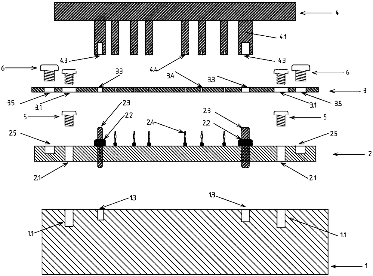
[0053] Such as figure 2 The explosion diagram of the crimping structure between the PCB board 3 and the IGBT module 2 is shown. On the basis of the embodiment 1, the position corresponding to the IGBT module screw 5 on the PCB board 3 is provided with a PCB board through hole 3.1, and The diameter of the PCB through hole 3.1 is larger than the nut diameter of the IGBT module screw 5 .

Embodiment 3

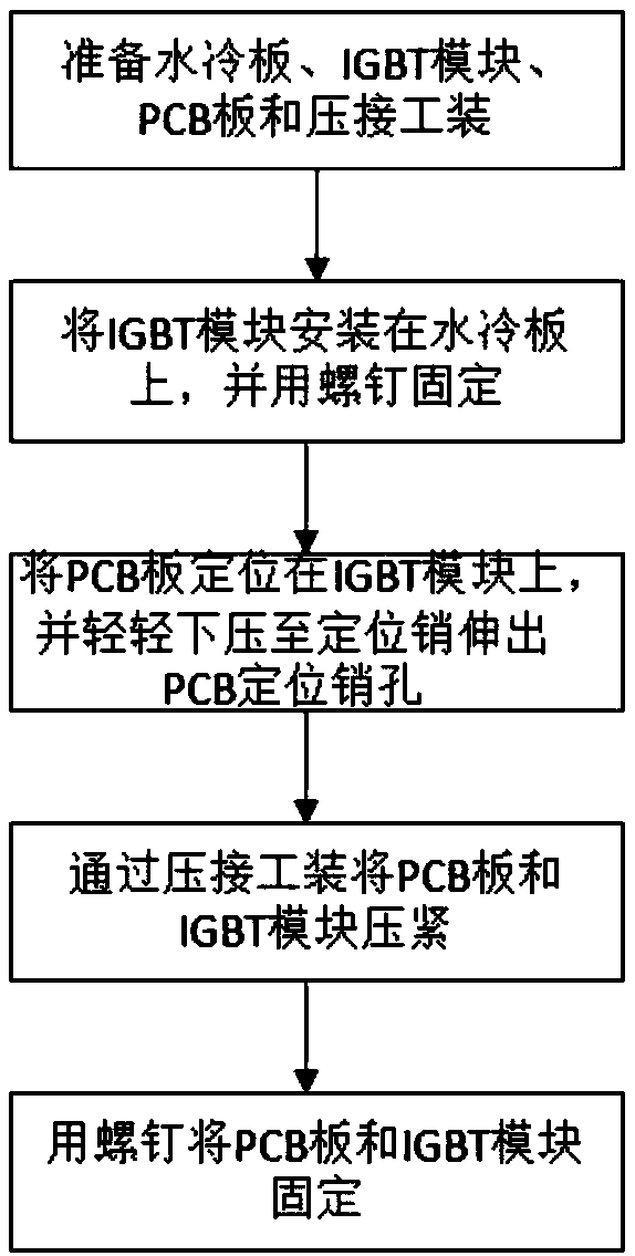
[0055] Such as figure 1 and 3 As shown, the embodiment of the present invention also provides a method for crimping a PCB board and an IGBT module, including the following steps:

[0056] Prepare the water-cooled plate 1, and drill out the water-cooled plate positioning pin hole 1.3 and the water-cooled plate threaded hole 1.1 on the water-cooled plate 1 in advance;

[0057] Prepare the IGBT module 2, pre-set the positioning pin 2.3 fixed on the IGBT module 2 and through the IGBT module 2 on the IGBT module 2, and fix a plurality of crimping pins 2.4 on the upper side of the IGBT module 2, so The IGBT module 2 is reserved with the IGBT module through hole 2.1 and the PCB board screw fixing hole 2.5 through the IGBT module screw, and the height-limiting boss 2.2 is set at the position of the IGBT module positioning pin 2.3, and the height-limiting boss 2.2 is close to the above the IGBT module 2;

[0058] Prepare the PCB board 3, reserve the PCB board crimping hole 3.4, the ...


PUM


Abstract

A PCB and IGBT module crimping structure and crimping method are disclosed, includes sequentially arranging water-cooled plate, IGBT module and PCB board from bottom to top, positioning water-cooled plate, IGBT module and PCB board by positioning pin, fixing water-cooled plate and IGBT module by screw, crimping PCB board and IGBT module by crimping tool and crimping pin and fixing with screw. Theinvention provides a PCB board and an IGBT module crimping structure and a crimping method, overcomes the defects of the prior art, and realizes high-quality and high-yield production of PCB and IGBTmodule assembly.

Description

technical field [0001] The invention relates to the technical field of microelectronics, in particular to a crimping structure and a crimping method of a PCB board and an IGBT module. Background technique [0002] At present, the process commonly used in the assembly of PCB and IGBT modules in automotive controllers is manual welding. Manual soldering is costly and inefficient. At the same time, the PCB is subject to the risks of temperature shock and mechanical deformation. And with the promulgation and implementation of the ROHS standard, the temperature requirements for lead-free soldering will be higher, and the quality of manual soldering will be more difficult to control. And maintenance disassembly is very troublesome. In the prior art, another commonly used process for assembling the PCB and the IGBT module in the automotive controller is a spring connection. This connection technology is a separable electrical connection. Contamination between separable connecte...

Claims


Application Information

Patent Timeline
IPC IPC(8): H05K1/02H05K1/18H05K3/30H01L23/40H01L23/473
CPCH01L23/4006H01L23/473H01L2023/4087H05K1/0203H05K1/184H05K3/306
Inventor 刘蕾葛贝贝苑红伟张红玉
Owner HEFEI JUYI POWER SYST CO LTD
Learn More