

Manufacture method for lithium niobate electro-optic device thick film traverse electrode
An electro-optical device and manufacturing method technology, applied in the field of optical communication, can solve the problems of large stress of thick film electrodes, waste of precious metals, etc., and achieve the effect of solving a lot of waste and overcoming excessive stress
- Summary
- Abstract
- Description
- Claims
- Application Information
AI Technical Summary
Problems solved by technology
Method used
Image

Examples
Embodiment 1
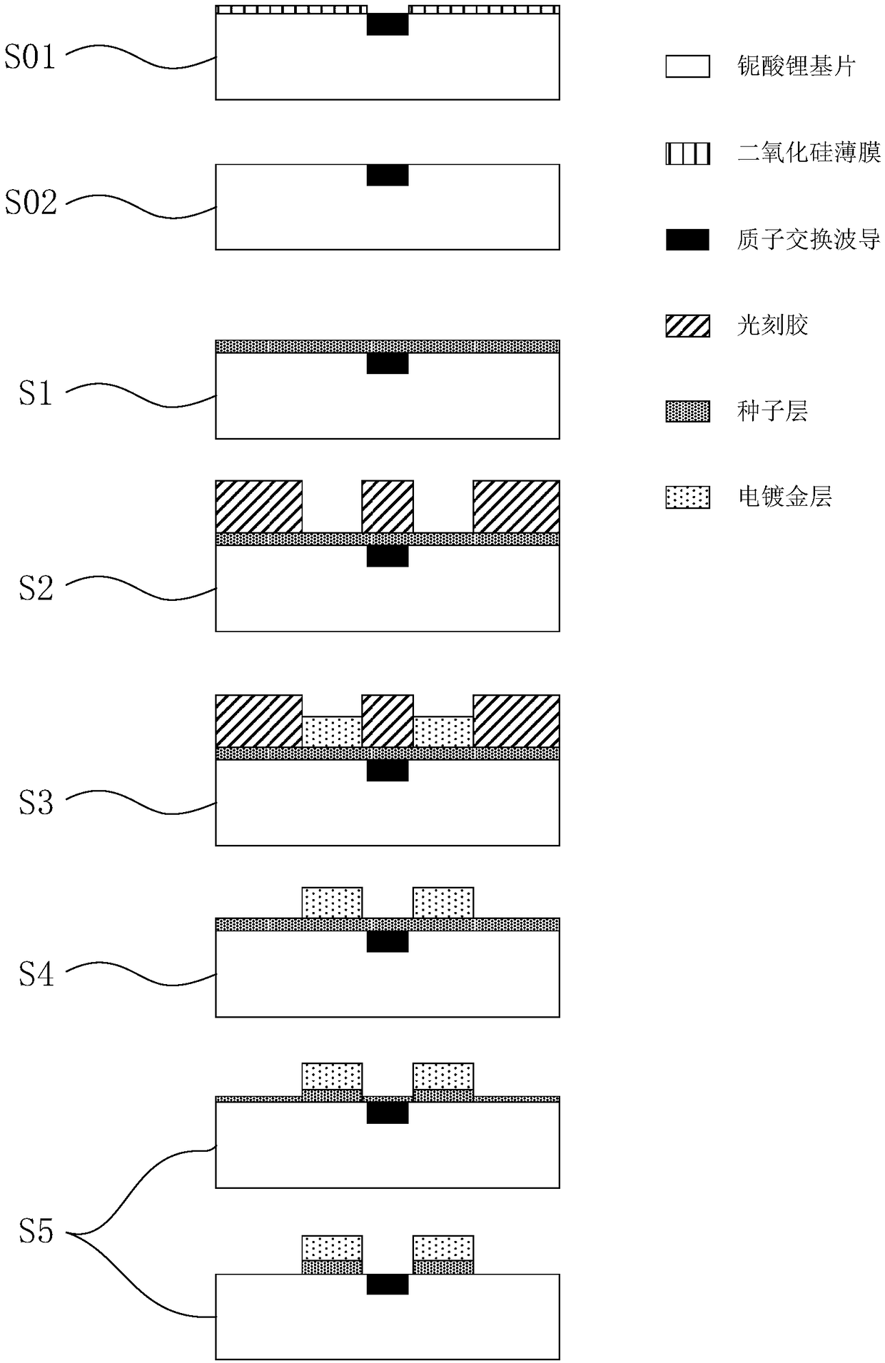
[0046] A method for manufacturing a thick-film wire electrode of a lithium niobate electro-optical device, comprising the following steps:
[0047] S1: Coating a metal seed layer on a lithium niobate substrate with a proton exchange waveguide to obtain a metallized substrate. The coating method is a plasma deposition method. The metal seed layer is divided into two layers, and the lower layer is adhesive The strength enhancement layer, the adhesion enhancement layer is nickel simple substance, the upper layer is a gold layer with a purity of not less than 99.99%, the thickness of the upper layer of the metal seed layer is 35nm, and the thickness of the lower layer of the metal seed layer is 15nm;
[0048] The preparation process of lithium niobate substrate with proton exchange waveguide is as follows:
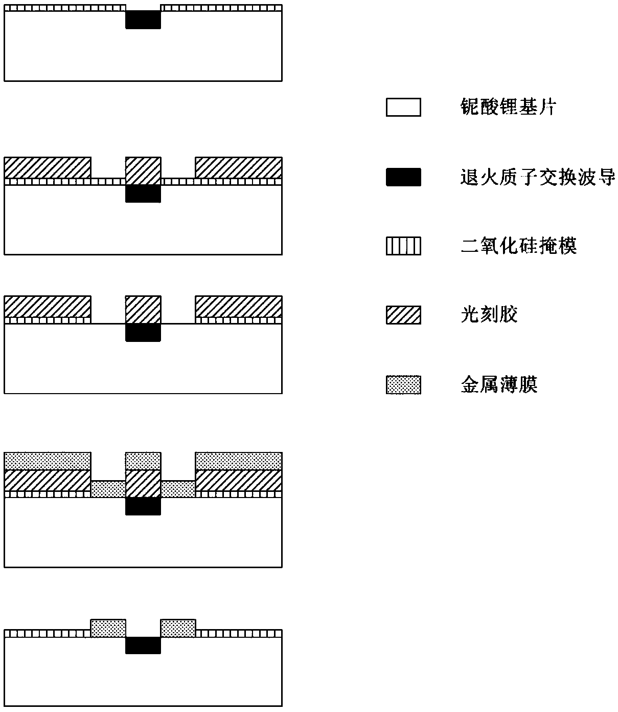
[0049] S01: Using silicon dioxide as a barrier layer, an optical waveguide is fabricated on the surface of a lithium niobate substrate by annealing proton exchange;
[0050] S0...
Embodiment 2
[0056] A method for manufacturing a thick-film wire electrode of a lithium niobate electro-optical device, comprising the following steps:
[0057] S1: Coating a metal seed layer on a lithium niobate substrate with a proton exchange waveguide to obtain a metallized substrate. The coating method is a physical vapor deposition method. The metal seed layer is divided into two layers, and the lower layer is for adhesion The strength enhancement layer, the adhesion enhancement layer adopts chromium element, the upper layer is a gold layer with a purity of not less than 99.99%, the thickness of the upper layer of the metal seed layer is 20nm, and the thickness of the lower layer of the metal seed layer is 10nm;
[0058] The preparation process of lithium niobate substrate with proton exchange waveguide is as follows:
[0059] S01: Using silicon dioxide as a barrier layer, an optical waveguide is fabricated on the surface of a lithium niobate substrate by annealing proton exchange; ...
Embodiment 3
[0066] A method for manufacturing a thick-film wire electrode of a lithium niobate electro-optical device, comprising the following steps:
[0067] S1: Coating a metal seed layer on a lithium niobate substrate with a proton exchange waveguide to obtain a metallized substrate. The coating method is magnetron sputtering. The metal seed layer is divided into two layers, and the lower layer is an adhesive layer. Adhesion enhancement layer, the adhesion enhancement layer is made of titanium element, the upper layer is a gold layer with a purity of not less than 99.99%, the thickness of the upper layer of the metal seed layer is 50nm, and the thickness of the lower layer of the metal seed layer is 20nm;
[0068] The preparation process of lithium niobate substrate with proton exchange waveguide is as follows:
[0069] S01: Using silicon dioxide as a barrier layer, an optical waveguide is fabricated on the surface of a lithium niobate substrate by annealing proton exchange;
[0070]...
PUM
| Property | Measurement | Unit |
|---|---|---|
| Thickness | aaaaa | aaaaa |
| Thickness | aaaaa | aaaaa |
| Thickness | aaaaa | aaaaa |
Abstract
Description
Claims
Application Information