

Preparation method of a conductive embolism and a semiconductor device with the conductive embolism
A conductive plug, semiconductor technology, applied in the direction of semiconductor devices, semiconductor/solid-state device manufacturing, semiconductor/solid-state device components, etc., can solve the problems of metal tungsten peeling, high tungsten plug resistance, affecting device reliability, etc., to eliminate voids Formation, void volume reduction, and high reliability effects
- Summary
- Abstract
- Description
- Claims
- Application Information
AI Technical Summary
Problems solved by technology
Method used
Image

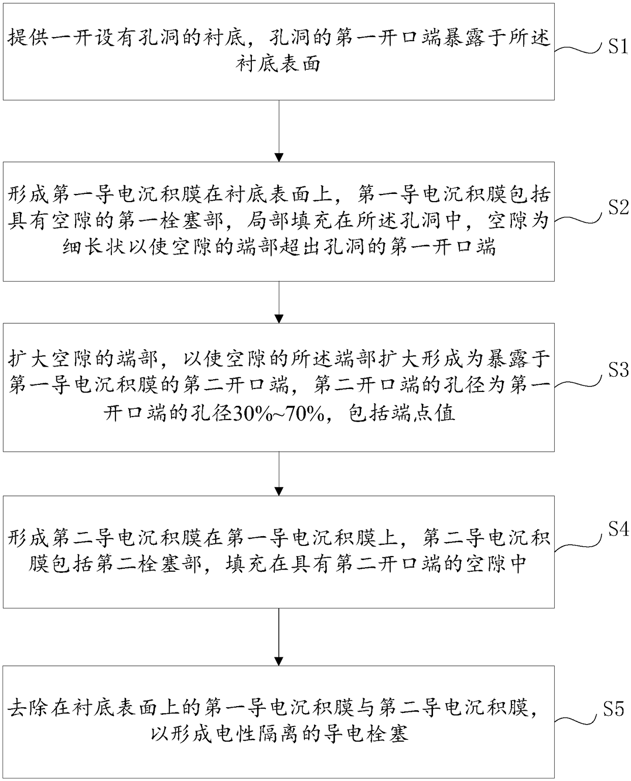
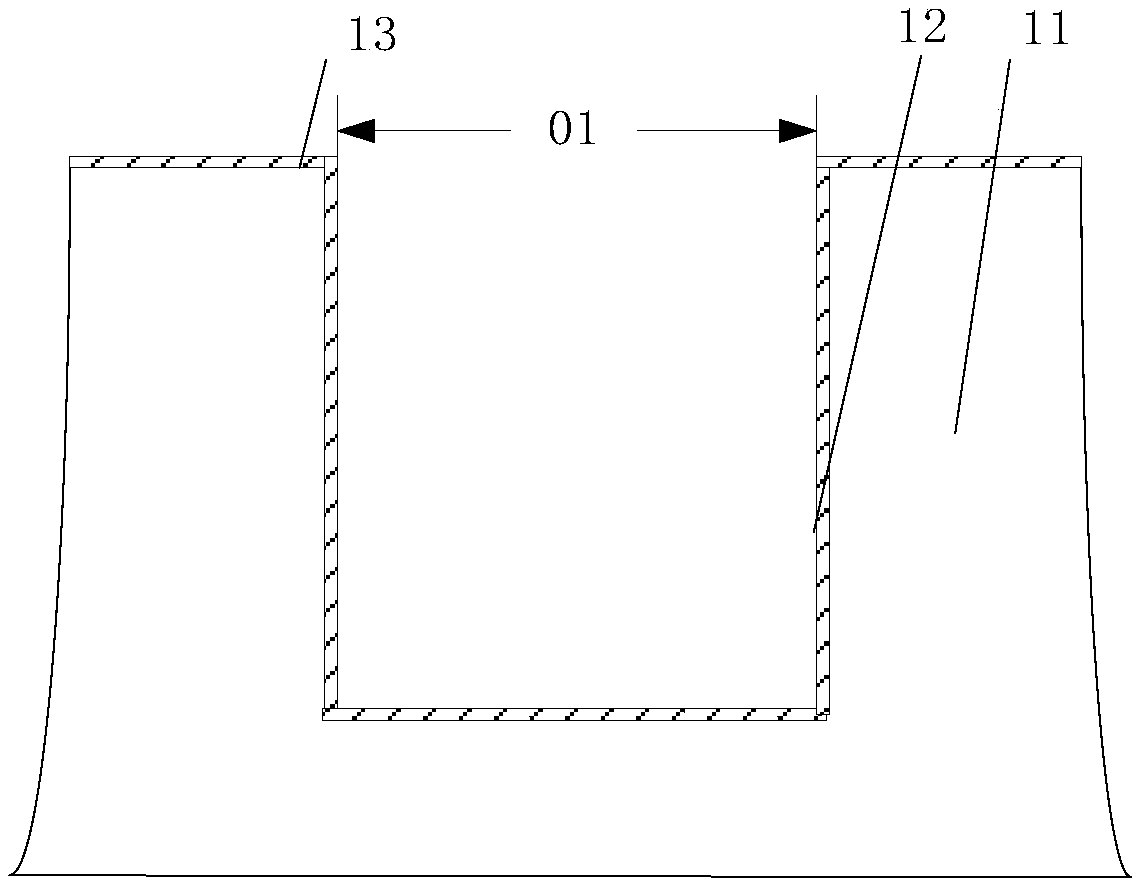
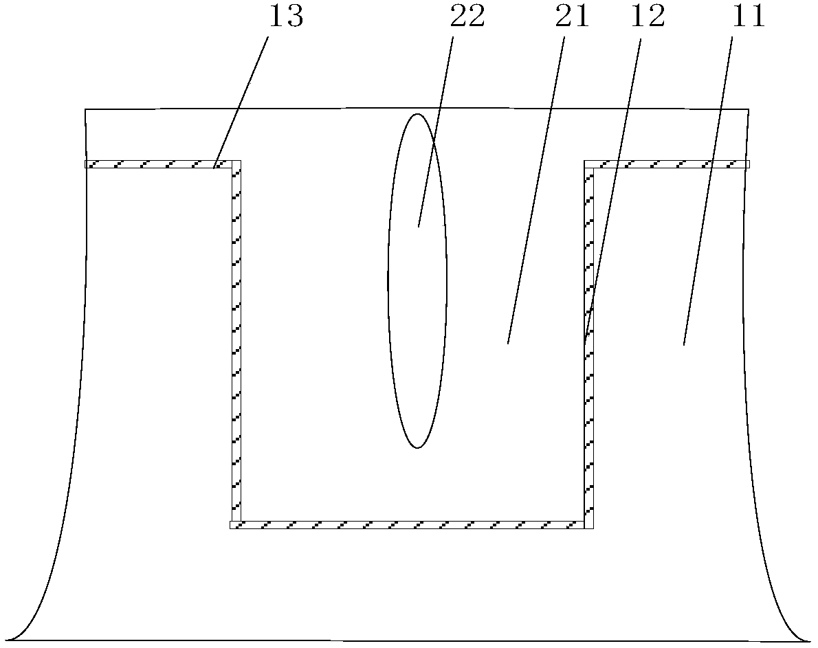
Examples
Embodiment Construction
[0053] In the following, only some exemplary embodiments are briefly described. As those skilled in the art would realize, the described embodiments may be modified in various different ways, all without departing from the spirit or scope of the present invention. Accordingly, the drawings and descriptions are to be regarded as illustrative in nature and not restrictive.
[0054] In describing the present invention, it is to be understood that the terms "center", "longitudinal", "transverse", "length", "width", "thickness", "upper", "lower", "front", " Back", "Left", "Right", "Straight", "Horizontal", "Top", "Bottom", "Inner", "Outer", "Clockwise", "Counterclockwise", etc. or The positional relationship is based on the orientation or positional relationship shown in the drawings, which is only for the convenience of describing the present invention and simplifying the description, rather than indicating or implying that the referred device or element must have a specific orie...
PUM
| Property | Measurement | Unit |
|---|---|---|
| pore size | aaaaa | aaaaa |
| depth | aaaaa | aaaaa |
| thickness | aaaaa | aaaaa |
Abstract
Description
Claims
Application Information