

Manufacturing method of Sip module with electromagnetic shielding structure and device
An electromagnetic shielding structure and electromagnetic shielding technology, applied in circuits, electrical components, electrical solid devices, etc., can solve the problems of high integration of Sip, large shielding slot size, and high fixture cost, and achieve small occupied space and production cost. The effect of low and low production cost
- Summary
- Abstract
- Description
- Claims
- Application Information
AI Technical Summary
Problems solved by technology
Method used
Image

Examples
specific Embodiment 1
[0035] combine Figure 1~5As shown, this specific embodiment discloses a method for manufacturing a SiP module with an electromagnetic shielding structure, including steps:
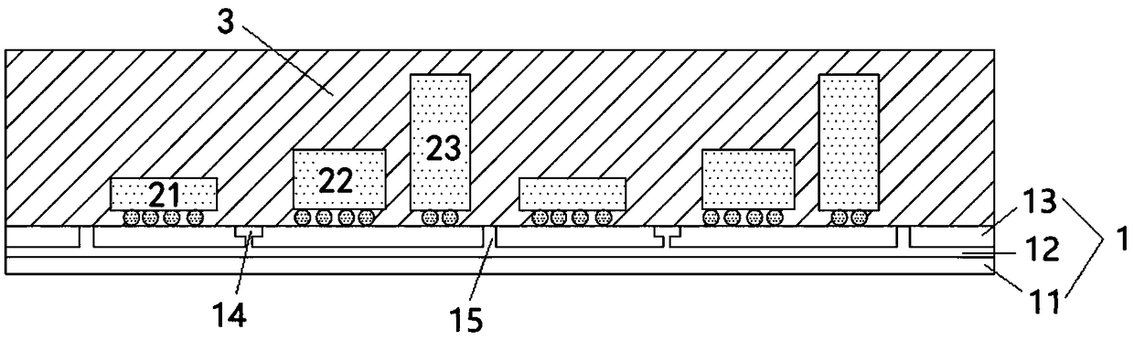
[0036] S1, making substrate 1, such as figure 1 As shown, the substrate 1 includes a support layer 11, a conductive layer 12, and an insulating layer 13 that are sequentially stacked from bottom to top. The substrate 1 is preset with a number of single SiP module layout areas and cutting for separating a single SiP module. In the insulating layer 13, a spacer conductive terminal 14 is provided in the layout area of a single SiP module. In the insulating layer 13, an edge conductive terminal 15 is arranged on the cutting track. The lower end surfaces of the spacer conductive terminal 14 and the edge conductive terminal 15 are respectively connected to the The conductive layer 12 is connected, and the upper end surfaces of the interval conductive ends 14 and the edge conductive ends 15 are exposed on the...
specific Embodiment 2
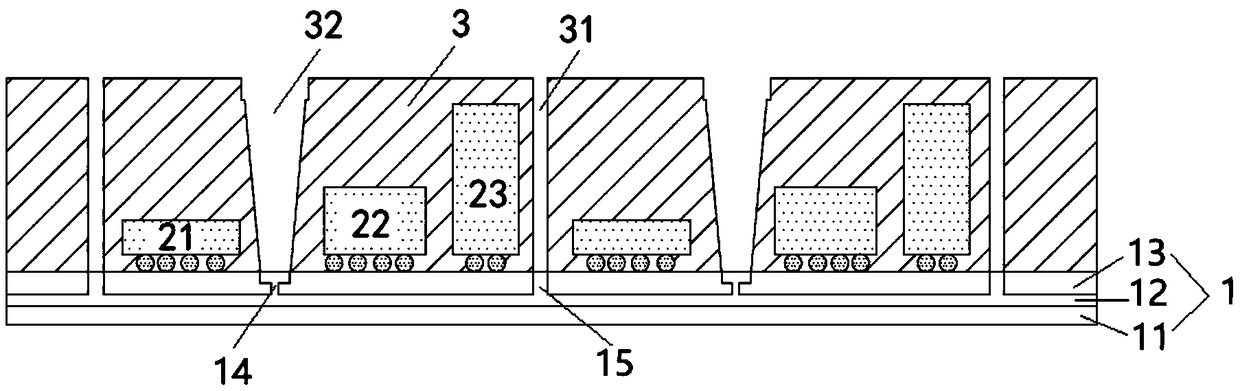
[0046] combine figure 1 , 2 As shown, this specific embodiment discloses a SiP module to be coated with electromagnetic shielding glue, including a substrate 1, a plurality of electronic components and a plastic sealing layer 3, the substrate 1 includes a support layer 11, which is stacked sequentially from bottom to top, The conductive layer 12 and the insulating layer 13, the substrate 1 is preset with a number of single SiP module layout areas and cutting lines for separating the single SiP module, and in the insulating layer 13, a single SiP module layout area is provided with a spaced conductive End 14, in the insulating layer 13, the edge conductive end 15 is set on the cutting line, the lower end surfaces of the spaced conductive end 14 and the edge conductive end 15 are respectively connected to the conductive layer 12, and the upper end surfaces of the spaced conductive end 14 and the edge conductive end 15 are connected to the substrate The upper end surface of 1 is...
specific Embodiment 3
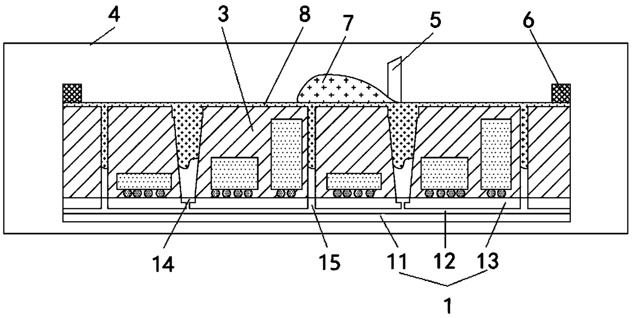
[0052] Such as image 3 As shown, this specific embodiment discloses an electromagnetic shielding glue coating device, which is used to implement the manufacturing method of the SiP module with an electromagnetic shielding structure in the specific embodiment one, including a vacuum chamber 4, a dispensing head (not shown in the figure) shown) and moving scraper 5, vacuum chamber 4 provides a vacuum environment for the SiP module to be coated with electromagnetic shielding glue, so that the common type shielding groove 31 and the interval shielding groove 32 in the SiP module to be coated with electromagnetic shielding glue Both are in a vacuum state, and the dispensing head is used to provide shielding glue 7 to the upper surface of the SiP module to be coated with electromagnetic shielding glue. The moving scraper 5 is located in the vacuum chamber 4. In the working state, the moving scraper 5 is located on the upper surface of the SiP module, and moves back and forth along ...
PUM
 Abstract
Description
Claims
Application Information