Packaged planar integrated gap waveguide dual-band filter

A dual-band filter and gap waveguide technology, applied in the field of electronics, can solve problems such as unpublished reports, and achieve the effects of good transmission performance, solving spatial resonance, and solving radiation loss and plane waves.

Inactive Publication Date: 2019-02-01
YUNNAN UNIV
View PDF0 Cites 3 Cited by
  • Summary
  • Abstract
  • Description
  • Claims
  • Application Information

AI Technical Summary

Problems solved by technology

[0005] Contents of the present invention, through literature search, do not see the public report identical with the present invention

Method used


Image

  • Packaged planar integrated gap waveguide dual-band filter
  • Packaged planar integrated gap waveguide dual-band filter
  • Packaged planar integrated gap waveguide dual-band filter

Examples


Embodiment Construction

[0034] The technical solution of the present invention will be further described in detail below in conjunction with specific embodiments.

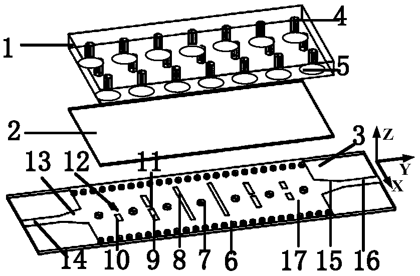
[0035] Such as Figure 1-6 As shown, the planar integrated gap waveguide dual-band filter packaged in the present invention includes: a top dielectric board (1), an intermediate dielectric board (2), and a bottom dielectric board (3), in which:

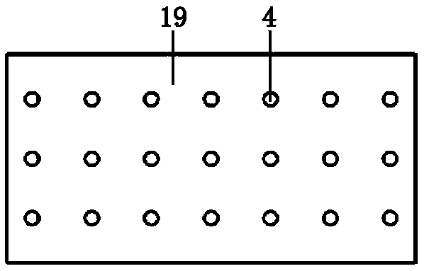
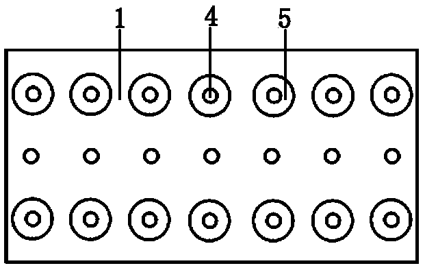
[0036] a. The upper surface of the top dielectric board (1) is printed with a metal layer (19), and the lower surface is printed with two rows of periodic metal circular patches (5); the top dielectric board (1) is printed in the direction parallel to the Y axis There are first periodic metal vias (4); the first periodic metal vias (4) have three rows: the two rows of periodic metal vias on both sides are located directly above the periodic metal round patch (5), The middle row of periodic metal vias is located in the middle of the top dielectric board;

[0037] b. The middle layer dielectric board (2...


PUM


Abstract

The invention relates to a packaged planar integrated gap waveguide dual-band filter, and the filter comprises three dielectric plates bonded together. The upper surface of the bottom dielectric plateis printed with a metal layer, and the metal layer is provided with a rectangular gap. Two ends of the metal layer are respectively connected with a transition gradual change line and a feed microstrip line, and the lower surface is printed with a grounding metal layer. Two sides and the center of the bottom dielectric plate are respectively provided with periodic metal via holes through perforation, thereby implementing an SIW filter. The upper surface of the top dielectric plate is printed with a metal layer, and the lower surface is printed with a metal circular patch, and the dielectric plate is provided with a periodic metal via hole through perforation, thereby forming an artificial magnetic conductor structure. The central dielectric plate separates the top dielectric plate and thebottom dielectric plate. According to the invention, the dual-band filter packaged through AMC is achieved, and the invention solves the problems of radiation loss and plane waves in a conventional filter. Meanwhile, the filter is small in gap, and is stable in structure.

Description

Technical field [0001] The invention relates to the field of electronic technology, in particular to a packaged planar integrated gap waveguide dual-band filter. Background technique [0002] Microwave multi-passband filters are a vital part of modern wireless communication systems. With the rapid development of microwave integrated circuits and the increasing shortage of spectrum resources, the entire system is developing in the direction of miniaturization and high performance. The performance and size of the filter put forward higher requirements. However, the early filters used simple parallel or cascaded connections, which greatly increased the size of the filter, and at the same time increased the transmission loss. [0003] The Substrate Integrated Waveguide (SIW) is a waveguide-like structure composed of a dielectric substrate, upper and lower metal surfaces, and metalized through holes. It also has the advantages of small size, low cost, easy processing and integration, w...

Claims


Application Information

Patent Timeline
Patent Type & Authority Applications(China)
IPC IPC(8): H01P1/20H01P1/203
CPCH01P1/20H01P1/203
Inventor 申东娅董明张秀普
Owner YUNNAN UNIV
Why Eureka
Try Eureka