Semiconductor device, manufacturing method thereof, and electronic equipment including the same

A technology for semiconductors and devices, applied in electronic equipment, vertical semiconductor devices and their manufacturing fields, can solve the problem of difficult gate length and relative position between gate and source and drain, difficulty in stacking multiple vertical devices, increasing channel resistance, etc. problem, to optimize switching performance, reduce leakage current, and reduce parasitic capacitance

Active Publication Date: 2022-04-19
INST OF MICROELECTRONICS CHINESE ACAD OF SCI
View PDF11 Cites 0 Cited by
  • Summary
  • Abstract
  • Description
  • Claims
  • Application Information

AI Technical Summary

Problems solved by technology

But for vertical devices, on the one hand, if polycrystalline channel materials are used, the channel resistance will be greatly increased, making it difficult to stack multiple vertical devices, because this will lead to excessively high resistance
On the other hand, if a single crystal channel material is used, there are problems such as difficult control of the gate length and the relative position of the gate and the source and drain.

Method used


Image

  • Semiconductor device, manufacturing method thereof, and electronic equipment including the same
  • Semiconductor device, manufacturing method thereof, and electronic equipment including the same
  • Semiconductor device, manufacturing method thereof, and electronic equipment including the same

Examples


Embodiment Construction

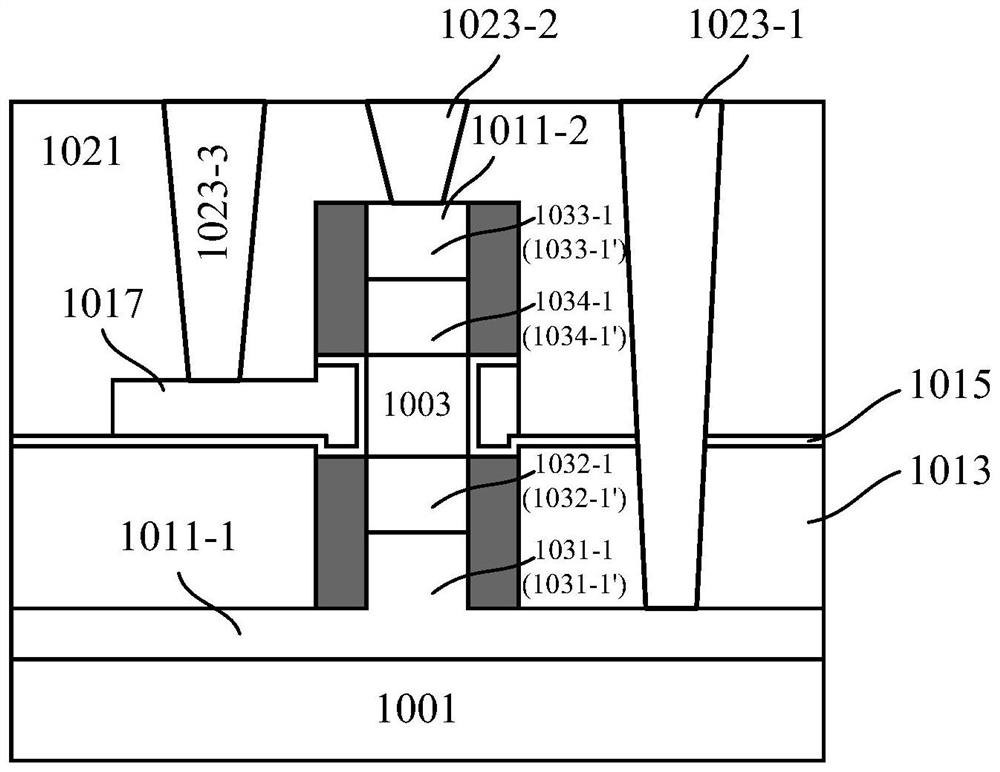
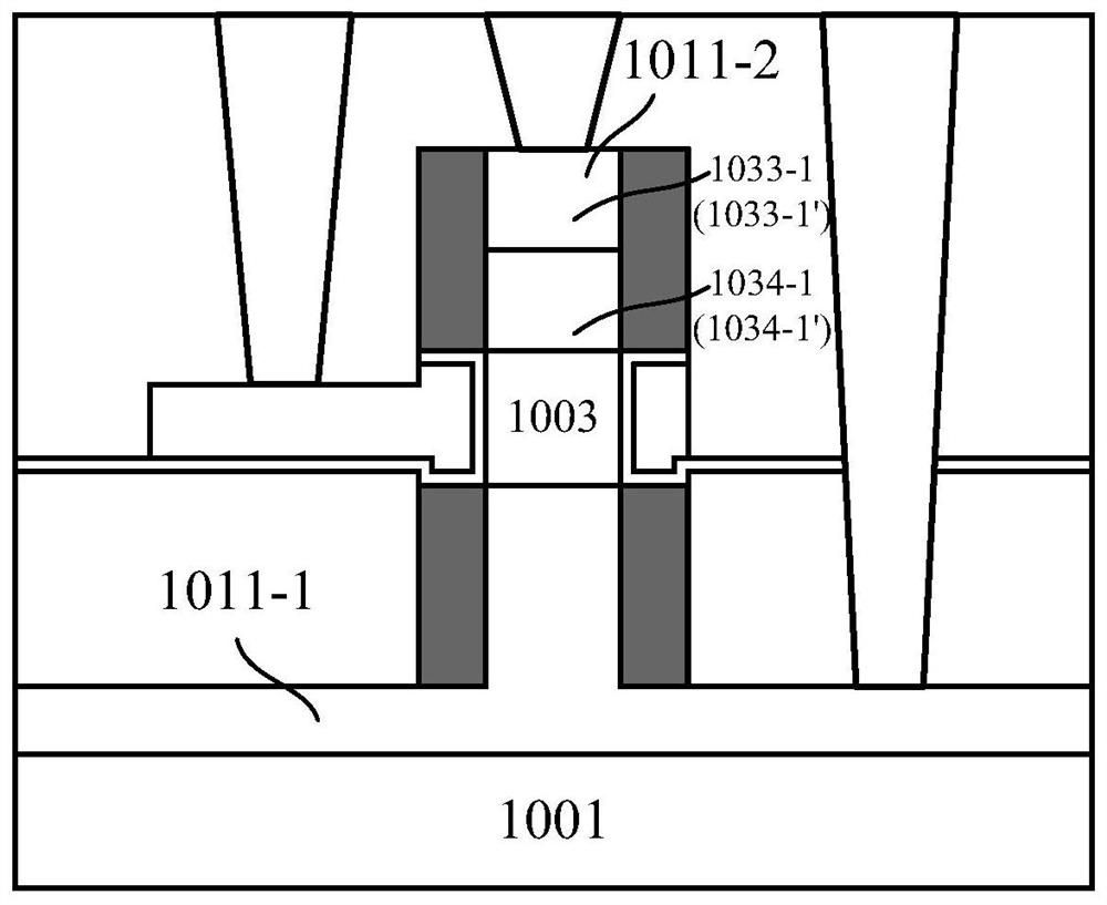
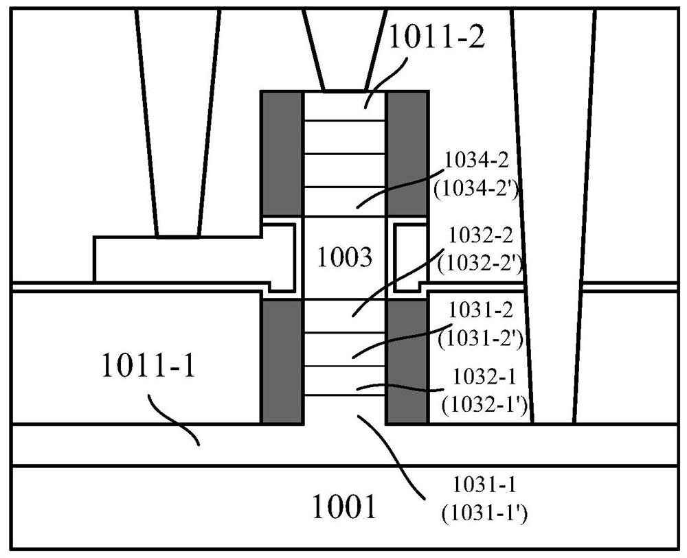
[0013] Hereinafter, embodiments of the present application will be described with reference to the drawings. However, it should be understood that these descriptions are only exemplary and not intended to limit the scope of the present application. Also, in the following description, descriptions of well-known structures and techniques are omitted to avoid unnecessarily obscuring the concept of the present application.

[0014] Various structural schematic diagrams according to embodiments of the present application are shown in the accompanying drawings. The figures are not drawn to scale, with certain details exaggerated and possibly omitted for clarity of presentation. The shapes of the various regions and layers shown in the figure, as well as their relative sizes and positional relationships are only exemplary, and may deviate due to manufacturing tolerances or technical limitations in practice, and those skilled in the art will Regions / layers with different shapes, siz...


PUM

PropertyMeasurementUnit
thicknessaaaaaaaaaa
thicknessaaaaaaaaaa
thicknessaaaaaaaaaa

Abstract

Disclosed are a semiconductor device, a manufacturing method thereof, and electronic equipment including the device. According to an embodiment, a semiconductor device may include: a substrate; a first source / drain layer, a channel layer, and a second source / drain layer sequentially stacked on the substrate and adjacent to each other, and a gate layer is formed around the periphery of the channel layer. Stacking; wherein, at least one interface structure is formed in at least one of the first source / drain layer and the second source / drain layer, and the conduction band energy level and / or the valence band energy level are different on both sides of the interface structure .

Description

technical field [0001] The present application relates to the field of semiconductors, in particular, to a vertical semiconductor device, a method for manufacturing the same, and an electronic device including the semiconductor device. Background technique [0002] Horizontal semiconductor devices such as metal oxide semiconductor field effect transistors (MOSFETs) are widely used in various electronic devices. In a horizontal MOSFET, the source, gate, and drain of the transistor are arranged in a direction roughly parallel to the top surface of the substrate, but this arrangement makes it difficult to further reduce the device area in the horizontal direction, thus affecting electronic equipment. The degree of integration increases the difficulty of further reducing manufacturing costs. [0003] In order to solve the above problems, vertical devices have been adopted. In a vertical type MOSFET, the source, gate, and drain of the transistor are arranged in a direction subs...

Claims


Application Information

Patent Timeline
Patent Type & Authority Patents(China)
IPC IPC(8): H01L29/78H01L29/06H01L29/08H01L29/423H01L21/336
CPCH01L29/0638H01L29/0847H01L29/42356H01L29/66666H01L29/7827H01L29/66545H01L29/267H01L29/161H01L29/201H01L29/2003
Inventor 朱慧珑吴振华
Owner INST OF MICROELECTRONICS CHINESE ACAD OF SCI
Why Eureka
Try Eureka