
Low-clamping protection device structure and manufacturing method thereof

A technology for protecting devices and manufacturing methods, which is applied in semiconductor/solid-state device manufacturing, electrical solid-state devices, semiconductor devices, etc., can solve the problems of IPP current capability decline, surge anti-surge capability, and high dissipation power, so as to reduce clamping voltage, increasing current capability, increasing the effect of inrush current

Pending Publication Date: 2019-02-15
无锡欣昱微电子有限公司
View PDF0 Cites 0 Cited by
  • Summary
  • Abstract
  • Description
  • Claims
  • Application Information

AI Technical Summary

Problems solved by technology

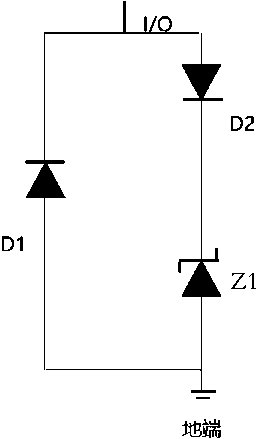
[0003] like figure 1 As shown, the existing integrated unidirectional low-capacitance TVS is usually composed of a low-capacitance PIN diode (D2) connected in series with an ordinary TVS, and then connected in parallel with a low-capacitance NIP diode (D1). Since the diodes D1 and D2 are formed by high-impedance epitaxy, As a result, the series resistance of itself is large, and the clamping voltage is very high, which will cause high power dissipation and be easily burned. data lost

Method used


Image

  • Low-clamping protection device structure and manufacturing method thereof
  • Low-clamping protection device structure and manufacturing method thereof
  • Low-clamping protection device structure and manufacturing method thereof

Examples


Embodiment Construction

[0039] The present invention will be further described below in conjunction with specific drawings and embodiments.

[0040] The embodiment of the present invention takes a P-type unidirectional low-capacitance TVS device as an example, the first conductivity type is P-type, and the second conductivity type is N-type.

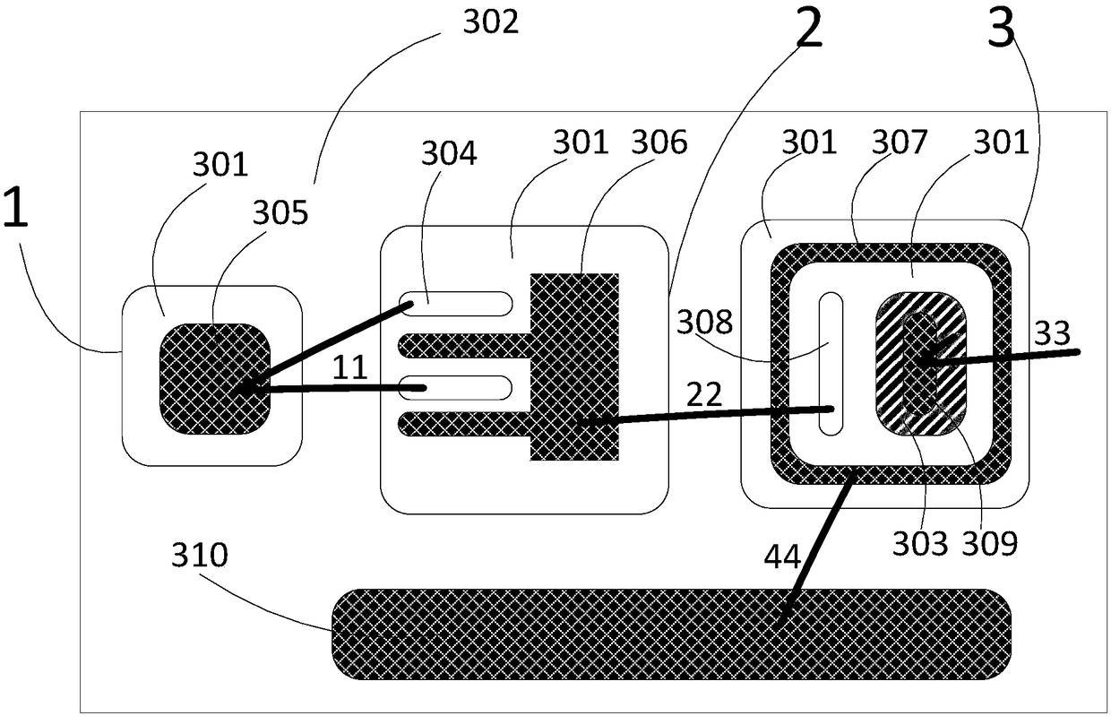
[0041] Such as image 3with Figure 5 As shown, a low-clamp protection device structure includes a P-type substrate 101 and an N-type epitaxial layer 301 located on the P-type substrate 101. It is characterized in that the device is arranged in the N-type epitaxial layer 301. A P-type isolation structure 302 divided into three regions, the P-type isolation structure 302 extending from the surface of the N-type epitaxial layer 301 into the P-type substrate 101;

[0042] A low-capacitance diode D1 for forming a device structure is provided in the first area 1, a low-capacitance diode D2 for forming a device structure is provided in the second area 2, and a disc...


PUM


Abstract

The invention belongs to the technical field of semiconductor protection devices, and relates to a low-clamping protection device structure and a manufacturing method thereof. A first conduction typeisolation structure which divides a device into three regions is arranged in a second conduction type epitaxial layer; a low-capacitance diode D1 is formed in the first region; a low-capacitance diodeD2 is formed in the second region; a discharge tube TSS is formed in the third region; a TVS voltage-stabilizing diode Z1 is formed in the first conduction type isolation structure; the TVS voltage-stabilizing diode Z1 is connected in parallel with the discharge tube TSS, and is connected with the diode D2 in series; the positive electrode of the diode D2 is connected with the negative electrodeof the TVS voltage-stabilizing diode Z1, and is connected with an I / O port; and the positive electrode of the diode Z1 is connected with the positive electrode of the diode D1 are grounded. By addingthe discharge tube TSS structure, on the basis of not enlarging the device area and increasing the process cost, a clamping voltage is reduced, and the current capacity is improved, so that the ESD capacity of a high-speed data transmission channel port is improved, the data integrity is guaranteed, and meanwhile burnout caused by excessively high dissipation power is prevented.

Description

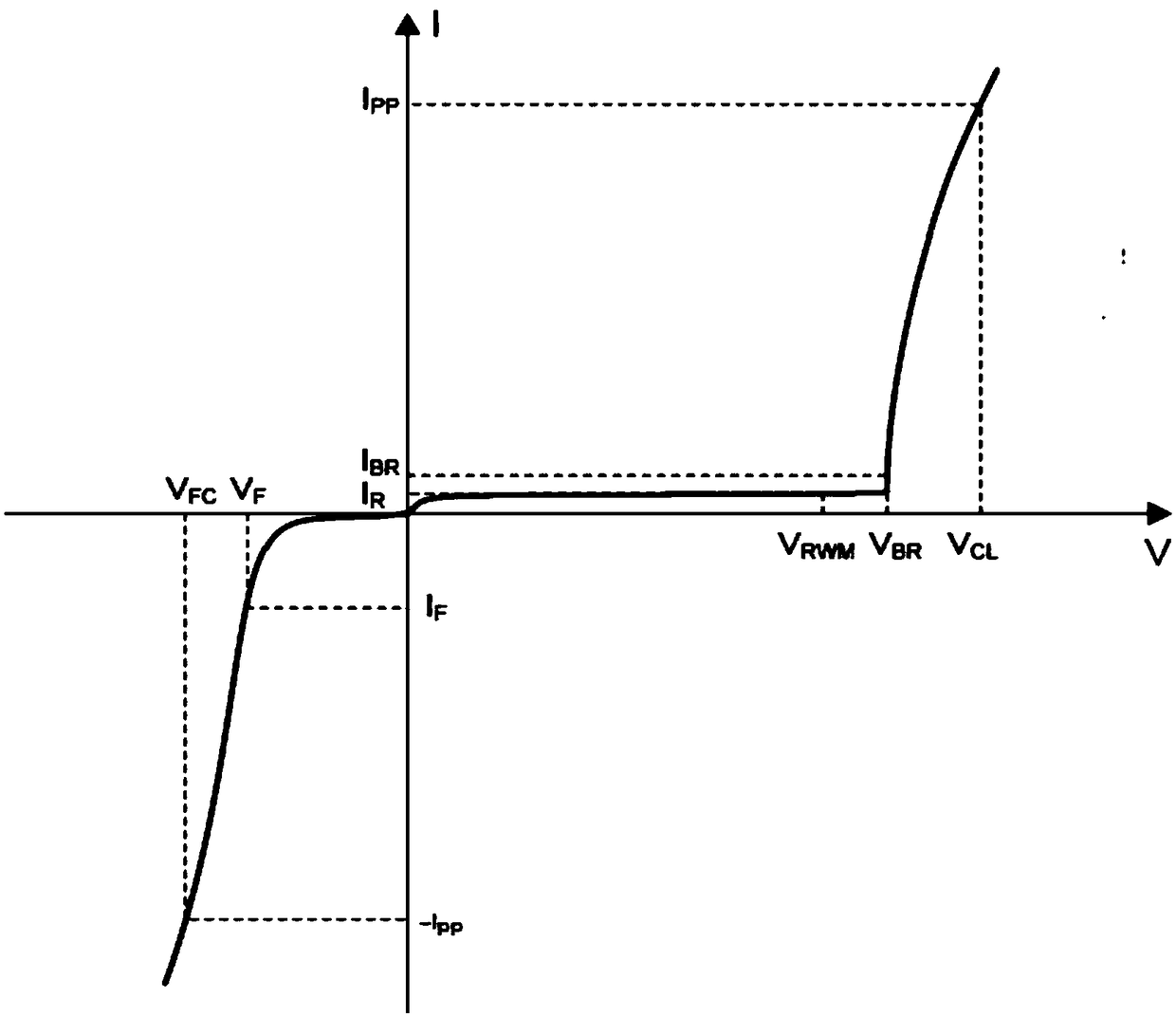
technical field [0001] The invention relates to a low-clamp protection device structure and a manufacturing method thereof, belonging to the technical field of semiconductor protection devices. Background technique [0002] Transient voltage suppressor (TVS) is widely used in the field of ESD protection, under the action of transient peak pulse current, such as figure 2 As shown, when the current flowing through TVS rises from the original reverse leakage current IR to IBR, the voltage presented at its two poles rises from the rated reverse turn-off voltage VRWM to the breakdown voltage VBR, and the TVS is broken down. With the appearance of the peak pulse current, the current flowing through TVS reaches the peak pulse current IPP. The voltage at its two poles is clamped below a predetermined maximum clamping voltage. Then, as the pulse current decays exponentially, the voltage at the two poles of the TVS also decreases continuously, and finally returns to the initial stat...

Claims


Application Information

Patent Timeline
Patent Type & Authority Applications(China)
IPC IPC(8): H01L27/02H01L29/06H01L21/8232
CPCH01L27/0207H01L27/0248H01L29/0603H01L29/0615H01L21/8232
Inventor 顾彦国
Owner 无锡欣昱微电子有限公司
Learn More