Chip of reverse blocking IGBT and manufacturing method

A chip and reverse resistance technology, which is applied in semiconductor/solid-state device manufacturing, electrical components, transistors, etc., can solve the problems of wide diffusion area of ​​P+ isolation area, waste of chip terminal area, long diffusion time, etc., and reduce the chip terminal area area, improve utilization rate, and reduce the effect of using area

Inactive Publication Date: 2019-02-15
BEIJING UNIV OF TECH
View PDF5 Cites 0 Cited by
  • Summary
  • Abstract
  • Description
  • Claims
  • Application Information

AI Technical Summary

Problems solved by technology

For the structural design of the traditional reverse resistance IGBT edge isolation region, see Figure 4A , using this diffusion isolation terminal design, the P+ isolation region is in contact with the bottom P+ is the difficulty of the entire structural design. It is easier to realize the low-voltage reverse resistance IGBT with a thinner substrate, but for higher withstand voltage and thicker substrate For high-voltage devices, it is more difficult to realize
The substrate of the high-voltage reverse resistance IGBT is thick and requires a long diffusion time. The P+ isolation area can be combined with the back P+. Due to the existence of lateral diffusion, the diffusion area of ​​the P+ isolation area is very wide, resulting in a large waste of chip terminal area.

Method used


Image

  • Chip of reverse blocking IGBT and manufacturing method
  • Chip of reverse blocking IGBT and manufacturing method
  • Chip of reverse blocking IGBT and manufacturing method

Examples


Embodiment 1

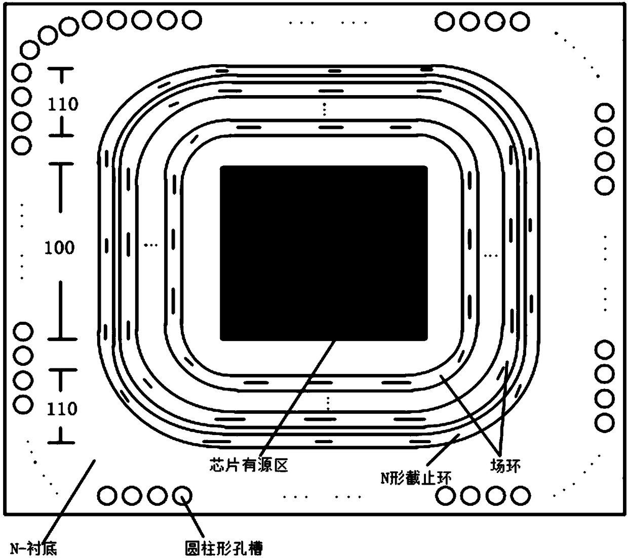
[0023] In this embodiment, a single-row cylindrical hole array is used, such as figure 1 As shown, the N-substrate doping concentration is 1e13cm -3 —5e13cm -3 , Thickness 400μm-550μm (depending on the size of the withstand voltage). The width of the active area of ​​the chip (100) is 200μm-400μm, the width of the terminal area (110) is 200μm-1000μm (depending on the withstand voltage), and the distance between the cylindrical holes is about 1μm-20μm (depending on the overall size of the chip) , the inner diameter of the cylindrical hole is 5μm-30μm (depending on the chip area), and the concentration of physical vapor deposition is 1e20cm -3 -5e20cm -3 B ion gas. Through experiments and simulation tests, when the same diffusion isolation region P+ is obtained, the diffusion time required by the present invention accounts for 1%-10% of the traditional diffusion method time. The chip edge area required by the structure is reduced by 80%-95%, thereby effectively reducing th...

Embodiment 2

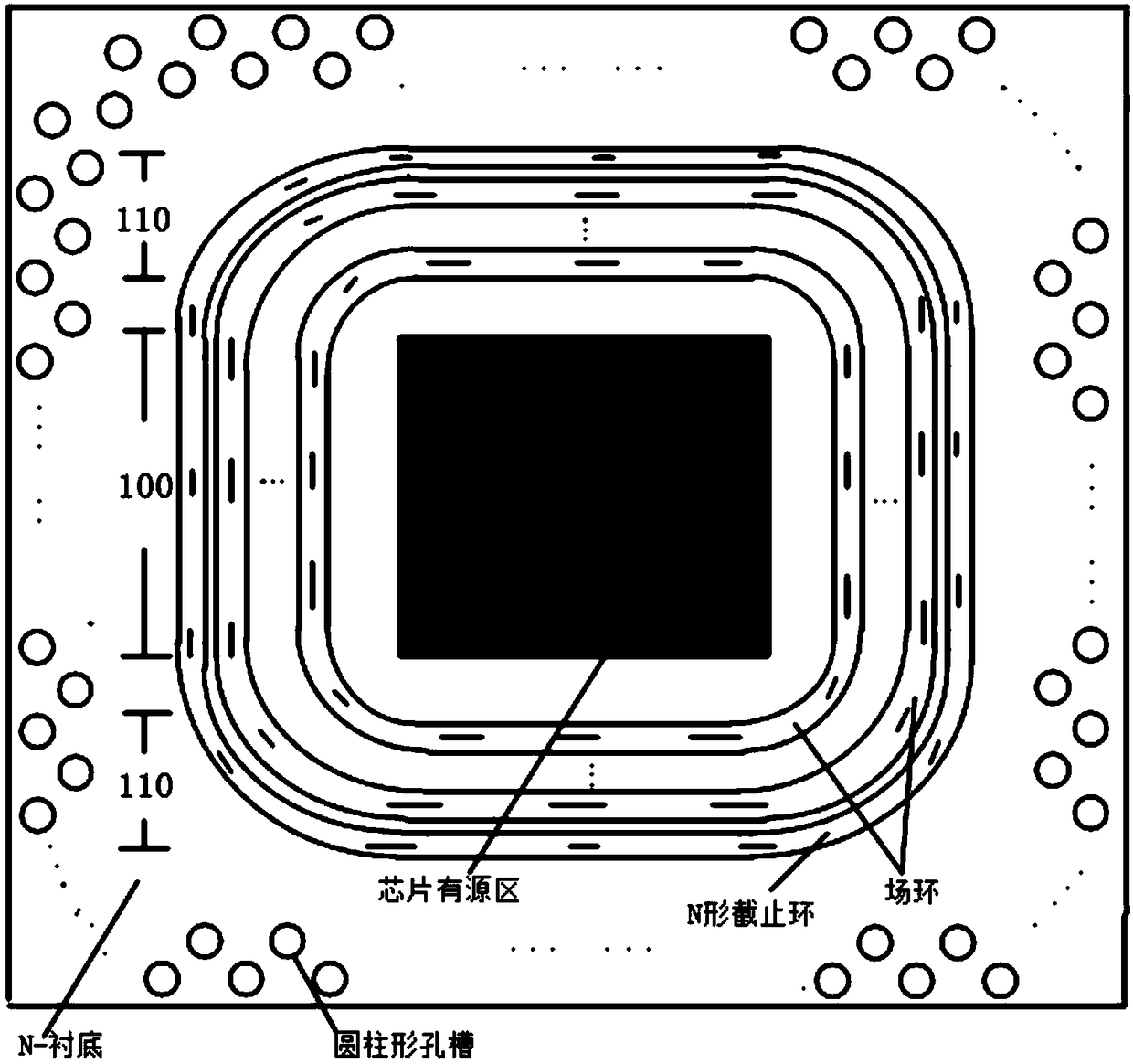
[0025] In this embodiment, a double-row isosceles triangular cylindrical hole array is used, such as figure 2 As shown, the N-substrate doping concentration is 1e13cm -3 —5e13cm -3 , Thickness 400μm-550μm (depending on the size of the withstand voltage). The width of the active area of ​​the chip (100) is 200 μm-400 μm, the width of the terminal area (110) is 200 μm-1000 μm (according to the size of the withstand voltage), and the distance between the outermost cylindrical holes is about 10 μm-20 μm (according to the overall size of the chip) fixed), the inner cylindrical hole and the outermost two cylindrical holes form an isosceles triangle, and the distance between the outermost cylindrical hole and the inner cylindrical hole is 1μm-10μm (the distance between the outermost hole and the outer hole The distance between), the inner diameter of the cylindrical hole is 5μm-30μm (depending on the chip area), and the concentration of physical vapor deposition is 1e20cm -3 -5e2...

Embodiment 3

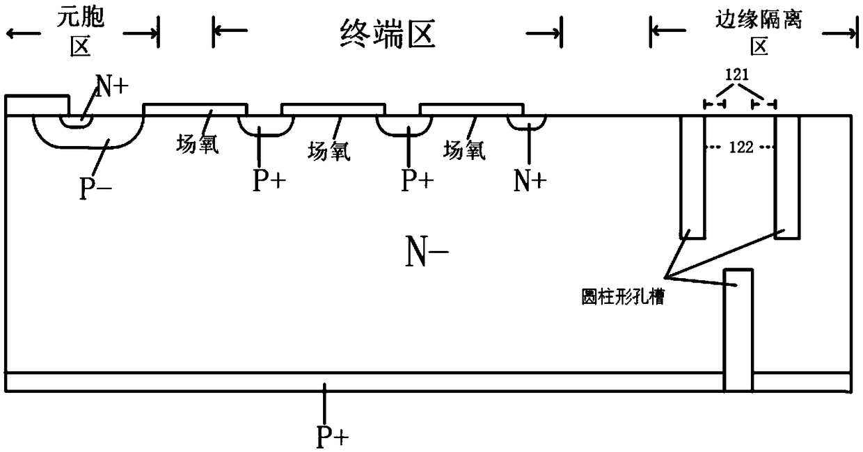
[0027] In this embodiment, a double-sided non-penetrating cross-cylindrical hole array is used, such as image 3 As shown in the chip section, the N-substrate doping concentration is 1e13cm -3 —5e13cm -3 , Thickness 400μm-550μm (depending on the size of the withstand voltage). The width of the active area of ​​the chip is 200μm-400μm, the width of the terminal area is 200μm-1000μm (according to the size of the withstand voltage), the distance between the cylindrical holes on the surface of the chip (122) is about 10μm-20μm, the back hole groove and the two holes on the surface The lateral distance (121) of the groove is 1 μm-10 μm, the inner diameter of the cylindrical hole is 5 μm-30 μm, the depth of the groove accounts for 40%-60% of the substrate thickness, and the concentration of physical vapor deposition is 1e20cm -3 -5e20cm -3 The B ion gas, the cross distribution of the cylindrical holes on the chip surface and the cylindrical holes on the bottom of the chip is show...


PUM


Abstract

The invention relates to a chip of a reverse blocking IGBT and a manufacturing method. According to the chip and the manufacturing method, hole grooves are formed in the edge of the chip to make contact with a collector P+ area on the back of the chip; and by adoption of physical gas deposition, the chip is put in gas which is full of boron ions to ensure that the boron ions are transversely diffused along the inner walls of the hole grooves until diffusion knots between the hole grooves make contact so as to form a diffusion and isolation area around a terminal area. Different from the conventional reverse blocking IGBT, the method adopts a diffusion method to manufacture the isolation area, so that the diffusion time is short, the operation is not influenced by the thickness of a substrate, the usable area of the isolation area is few and the chip area utilization rate is high. The bottoms of the hole grooves make contact with the collector P+ area on the back, so that the difficultythat the bottom of the diffusion and isolation area is difficult to make contact with the collector on the back as the substrate of a high-voltage device is relatively thick, and the diffusion knotsbetween the hole grooves make contact to form the overall diffusion P+ area so that the terminal area of the chip is isolated from the edge of the chip and then the edge of the chip is avoided from leakage current generation.

Description

Technical field: [0001] The invention relates to the structure of a power semiconductor device in the field of semiconductor technology, and the design of the structure design of the reverse resistance IGBT terminal isolation region. Background technique [0002] Conventional IGBT in order to compromise the on-state voltage drop V on and turn-off loss E off , typically with a buffer layer for smaller V on and E off , because the doping concentration of the buffer layer and the collector layer is very high, and the edge of the chip will cause a large leakage current due to lattice damage and stress, so the conventional IGBT does not have reverse blocking capability. The anti-resistance IGBT adopts the traditional non-punch-through (NPT) structure, and at the same time, it has been improved on the back and side, and an effective edge isolation area P+ is designed at the edge of the chip, so that the edge isolation area P+ and the back P+ area are short-circuited. Avoid the...

Claims


Application Information

Patent Timeline
IPC IPC(8): H01L29/739H01L29/06H01L21/331
CPCH01L29/0607H01L29/66333H01L29/7395
Inventor 吴郁何紫东龚超
Owner BEIJING UNIV OF TECH
Why Eureka
Try Eureka