Fluorescence enhanced chip based on all-medium artificial microstructure super-surface

An artificial microstructure and fluorescence enhancement technology, applied in fluorescence/phosphorescence, material excitation analysis, etc., can solve the problems of reduced fluorescence efficiency and large material loss, and achieve the effects of improving detection sensitivity, reducing material loss, and flexible structural design

Pending Publication Date: 2019-02-22
ZHEJIANG UNIV
View PDF10 Cites 7 Cited by
  • Summary
  • Abstract
  • Description
  • Claims
  • Application Information

AI Technical Summary

Problems solved by technology

However, metals have a large material loss in the visible and near-infrared bands, especially when the fluorescent marker is too close to the metal structure (less than 15 nanometers), its fluorescence efficiency will be greatly reduced, this phenomenon is also called fluorescence quenching

Method used


Image

  • Fluorescence enhanced chip based on all-medium artificial microstructure super-surface
  • Fluorescence enhanced chip based on all-medium artificial microstructure super-surface
  • Fluorescence enhanced chip based on all-medium artificial microstructure super-surface

Examples


Embodiment 1

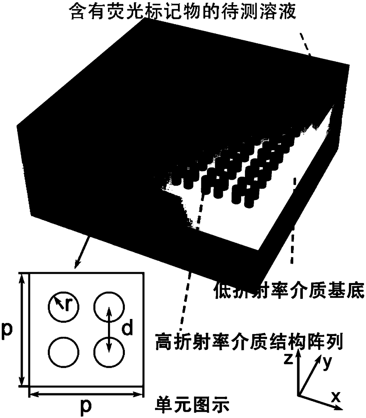
[0038] This embodiment is a chip for enhancing fluorescent signal for an up-conversion fluorescent marker (NaYF4:Yb / Tm) with an excitation wavelength of 965nm and a radiation wavelength of 800nm. Silicon (Si) is used as the material of the nano-dielectric column, while the substrate is a quartz glass material (SiO2). The entire chip is submerged in water. The design parameters are as follows:

[0039] p=520nm, t=270nm, r=68nm, d=200nm

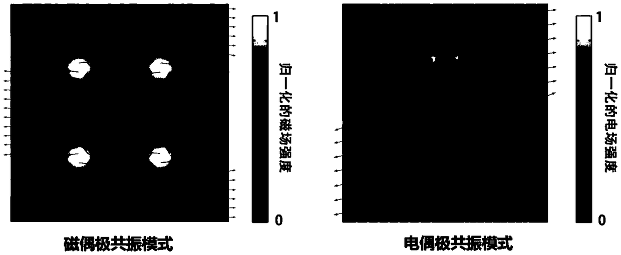
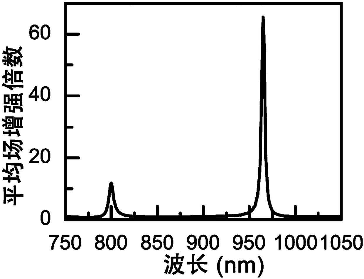
[0040] Through numerical simulation, we can get the average local field enhancement spectrum at 40nm above the chip as image 3 shown. It can be observed that there are two field enhancement peaks at wavelengths of 800 nm and 965 nm, which correspond to collective magnetic dipole resonance and electric dipole resonance, respectively. Adjusting the height of the silicon pillar can change the position of the second resonance peak, and adjusting the radius of the silicon pillar can change the positions of the two resonance peaks at the same ti...


PUM

PropertyMeasurementUnit
refractive indexaaaaaaaaaa

Abstract

The invention discloses a fluorescence enhanced chip based on an all-medium artificial microstructure super-surface. An upper layer of the chip is composed of periodically-arranged nano-medium columnclusters, and a lower layer is a medium substrate; the refractive index of the upper layer is greater than that of the lower layer; the collective magnetic dipole resonance wavelength and the collective electric dipole resonance wavelength of the chip satisfy that one is equal to the excitation wavelength of a fluorescent marker, and the other is equal to the radiation wavelength of the fluorescent marker. In the periodically-arranged nano-medium column clusters, each of periodic units is a square or a regular hexagon of the same size; four nano-medium columns of the same size are contained ineach of the periodic units. The fluorescence enhanced chip disclosed by the invention has the benefits that a fluorescence signal is simultaneously enhanced from three aspects of enhancing an excitation light local field, improving the radiation quantum efficiency and improving the fluorescence collection efficiency, so that the detection sensitivity of the fluorescent marker is greatly improved.The whole chip is arranged on a low-refractive index substrate and has the advantages that the material loss is low, the preparation is simple, and the structure size can be changed to work in different wavebands.

Description

technical field [0001] The invention belongs to the field of surface-enhanced fluorescence signals, and in particular relates to a fluorescence-enhanced chip based on an all-dielectric artificial microstructure metasurface, which is mainly used for detecting substances marked by fluorescent molecular groups, identifying substances, and analyzing the properties of substances. Under the excitation of visible light or near-infrared light source, the fluorescence enhancement chip expresses in the form of visible and near-infrared light through the process of up-conversion or down-conversion fluorescence, and can realize rapid and sensitive qualitative and quantitative detection of the sample to be tested. Background technique [0002] In molecular biology, biochemistry, protein chip technology and other life science fields, people often use fluorescent markers to achieve quantitative and qualitative detection of specific substances (such as nucleic acids, antigens, enzymes, etc.)...

Claims


Application Information

Patent Timeline
Patent Type & Authority Applications(China)
IPC IPC(8): G01N21/64
CPCG01N21/64
Inventor 何赛灵龚晨晟
Owner ZHEJIANG UNIV
Why Eureka
Try Eureka