Solder mask manufacturing process for PCBs applied to LED display screens

A technology of LED display and PCB board, applied in printed circuit manufacturing, secondary processing of printed circuit, electrical components, etc., can solve the problem of LED light board easily producing ink color

Active Publication Date: 2019-03-01
东莞市若美电子科技有限公司
View PDF16 Cites 8 Cited by
  • Summary
  • Abstract
  • Description
  • Claims
  • Application Information

AI Technical Summary

Problems solved by technology

[0003] In view of this, the present invention aims at the deficiencies of the existing technology, and its main purpose is to provide a PCB board solder-proof manufacturing proc...

Method used


Image

  • Solder mask manufacturing process for PCBs applied to LED display screens
  • Solder mask manufacturing process for PCBs applied to LED display screens

Examples


Embodiment Construction

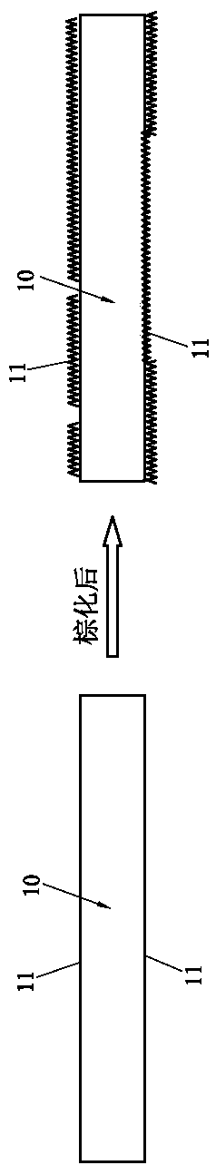
[0025] Please refer to figure 1 and figure 2 As shown, it discloses a PCB board solder mask manufacturing process for LED display applications, including the following steps:

[0026] (1) Pre-treatment: The surface of the PCB board 10 is treated by a browning process to increase the roughness of the copper surface 11 of the PCB board 10 and the roughness is uniform; specifically, the surface of the PCB board 10 is removed by acid and alkali washing Oxide, oil and fingerprints and other foreign matter, together with the liquid medicine of the activation tank and the browning tank, will chemically react the copper surface 11 of the PCB board 10 .

[0027] (2) Silk screen printing: Silk screen printing is performed on the copper surface 11 of the PCB board 10. During the silk screen printing process, the viscosity of the ink, the angle of the squeegee, the amount of ink scraped by the squeegee, and the speed of the squeegee are strictly controlled. After the silk screen, the st...


PUM


Abstract

The invention discloses a solder mask manufacturing process for PCB applied to LED display screens. The process comprises the following steps of: (1) preprocessing: processing the surface of a PCB byadoption of a browning process; (2) silk printing: carrying out silk printing on a copper surface of the PCB, strictly controlling an ink opening viscosity of printing ink, an angle of a doctor blade,an ink scraping amount of the doctor blade and a speed of the doctor blade in the silk printing process, and carrying out standing for 15-30 min after the silk printing; (3) pre-baking; (4) exposure;(5) development; (6) appearance inspection; (7) micro erosion; and (8) ink color check. According to the process, the solder mask preprocessing manner is the browning process, so that the copper surface can be uniformly coarsened; silk printing parameters, exposure parameters and development parameters are controlled at optimum values, so that solder mask windowing analysis is smooth after the development of the PCB; and after the development, the browned layer on the windowed copper surface is removed through micro erosion, so that the copper surface is better is flatness and color, the appearance ink color of the PCB is consistent, and the ink color problems caused by unfavorable solder mask exposure and bad solder mask analysis can be effectively solved.

Description

technical field [0001] The invention relates to the technology in the field of PCB board production, in particular to a PCB board welding-proof manufacturing process for LED display screens. Background technique [0002] The current method is to adopt the ordinary solder mask production process. The pre-treatment of solder mask is needle brush, needle brush + volcanic ash, needle brush + super roughening, etc. The silk screen and exposure stations are common process technical parameters, which are easy to produce PCB The problem of ink color on the board, especially for LED light boards with a COB package and a pitch below P2.0, the ink color problem is more serious, which eventually leads to poor display effects after LED light mounting. Therefore, it is necessary to improve the current solder mask manufacturing process. Contents of the invention [0003] In view of this, the present invention aims at the deficiencies of the existing technology, and its main purpose is t...

Claims


Application Information

Patent Timeline
IPC IPC(8): H05K3/28
CPCH05K3/282H05K2203/052
Inventor 洪少鸿
Owner 东莞市若美电子科技有限公司
Why Eureka
Try Eureka