Packaging film and application thereof

A technology for encapsulating thin films and forming films, which is applied in the direction of electrical components, circuits, and electric solid devices, etc., can solve the problems of unsatisfactory packaging film layer stability, poor performance stability of electronic devices, and poor barrier ability, etc., to achieve the stability of inorganic substances Good, good compactness, increase the effect of interface adhesion

Inactive Publication Date: 2019-03-05
TCL CORPORATION
View PDF6 Cites 4 Cited by
  • Summary
  • Abstract
  • Description
  • Claims
  • Application Information

AI Technical Summary

Problems solved by technology

[0011] The purpose of the present invention is to overcome the above-mentioned deficiencies in the prior art, and provide a packaging film to solve the technical problems of unsatisfactory stability and poor water and oxygen barrier ability of existing organic polymers as electronic component packaging films.
[0012] Another object of the present invention is to provide an electronic device and its preparation method to solve the technical problems of poor performance stability and unsatisfactory service life of the existing electronic device due to factors such as poor water and oxygen barrier properties of the packaging member and unstable structure.

Method used


Image

  • Packaging film and application thereof
  • Packaging film and application thereof
  • Packaging film and application thereof

Examples


preparation example Construction

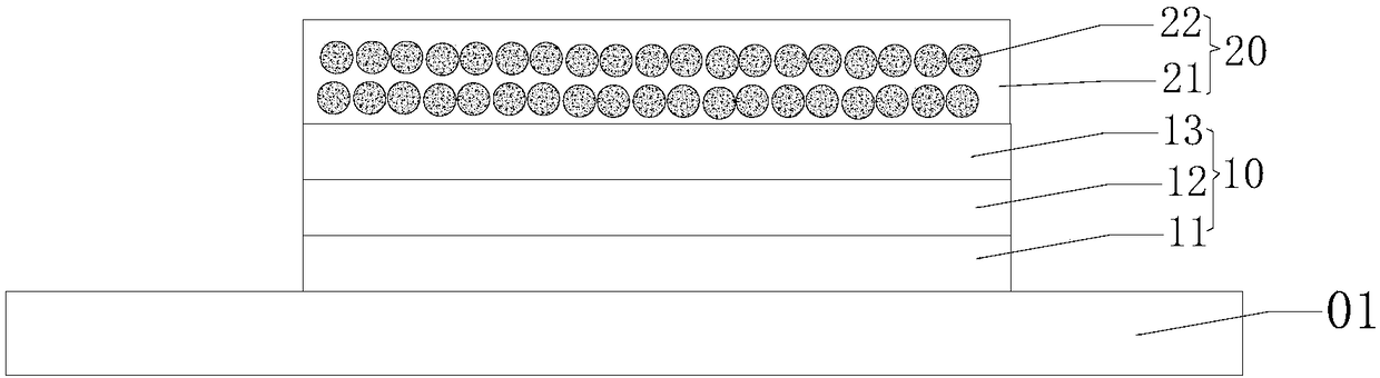
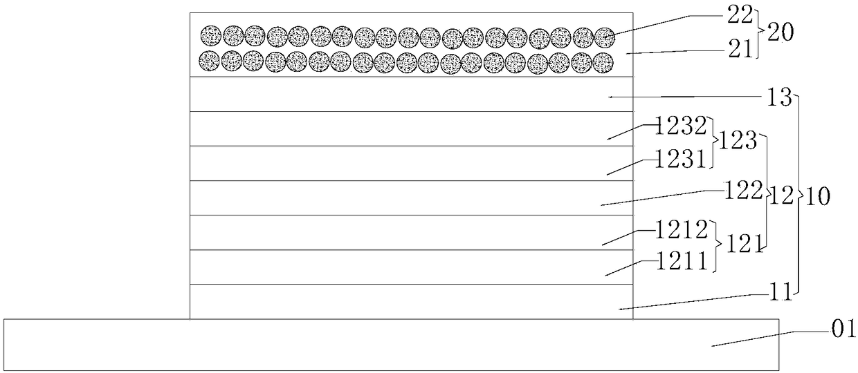
[0062] In another aspect, an embodiment of the present invention provides a method for manufacturing the electronic device. Combine Figure 1-3 , The manufacturing method of the electronic device includes the following steps:

[0063] Providing a substrate, the substrate including a substrate 01 and an electronic component 10 disposed on the substrate;

[0064] The packaging film 20 is formed on the substrate to encapsulate the electronic components.

[0065] The term "encapsulation" used in the present invention refers to the use of an encapsulation film to cover the parts of the electronic components that need to be encapsulated. According to the realized characteristics or work needs, different electronic component 10 structures have different requirements for the encapsulated parts. Specifically, The portion of the electronic component 10 that needs to be packaged can be all the top surfaces and sides of the electronic component, or of course, it can also be only the top surfac...

Embodiment 1

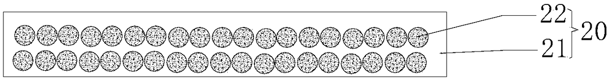
[0085] This embodiment provides an electronic device. It includes a substrate, a QLED electronic component bonded on the substrate, and a packaging film for packaging the QLED electronic component. The structure of the electronic device is: ITO substrate / PEDOT:PSS (50nm) / poly-TPD (30nm) / quantum dot light-emitting layer (20nm) / ZnO (30nm) / silver (70nm) / encapsulation film (700nm). Wherein, the material of the packaging film is SiO 2 Nanoparticles and polysiloxane composite, the SiO 2 Nano particles are dispersed in polysiloxane, and SiO 2 Nanoparticles are 1.5% of the mass of the packaging film, and the thickness of the packaging film is 700 nm.

[0086] The electronic device of this embodiment is prepared according to the following method:

[0087] S11: The layers are sequentially formed on the ITO substrate according to the QLED structure of this embodiment to form a QLED;

[0088] S12: Screen printing is used to form a packaging film on the top surface of the silver electrode of th...

Embodiment 2

[0093] This embodiment provides an electronic device. It includes a substrate, a QLED electronic component bonded on the substrate, and a packaging film for packaging the QLED electronic component. The structure of the electronic device is: ITO substrate / PEDOT:PSS (50nm) / poly-TPD (30nm) / quantum dot light-emitting layer (20nm) / ZnO (30nm) / silver (70nm) / encapsulation film (1000nm). Wherein, the material of the packaging film is SiO 2 Nanoparticles and polysiloxane composite, the SiO 2 Nano particles are dispersed in PTFE, and SiO 2 The nanoparticles account for 4.8% of the mass of the packaging film, and the thickness of the packaging film is 1000 nm.

[0094] The preparation method can refer to the method in Example 1, only need to adjust the SiO in the colloid 2 The content of squeegee should be adjusted, and the value of the squeegee pressure should be about 110N / m, the squeegee angle should be 60°, the curing temperature should be 120°C, and the curing time should be 40min.


PUM

PropertyMeasurementUnit
contact angleaaaaaaaaaa
thicknessaaaaaaaaaa
particle diameteraaaaaaaaaa

Abstract

The invention discloses a packaging film, and a preparation method and application thereof. The packaging film of the present invention comprises a polymer and inorganic nanoparticles dispersed in thepolymer. The packaging film of the invention has the advantages of good stability and high-temperature resistance of inorganic matter and good film-forming property and flexibility of organic matter;and the organic polymer and the inorganic nanoparticle component are closely mixed with each other to form a new form, and thus the film has better compactness, can better block penetration of waterand oxygen, ensures the stability of electrochemical performance of packaged electronic components, and extends the working life of electronic components. The preparation method of the packaging filmensures the structural stability of the packaging film and excellent water-proof and oxygen-proof performance. The application of the film includes application to electronic devices.

Description

Technical field [0001] The invention belongs to the technical field of encapsulation films, and specifically relates to an encapsulation film, an electronic device containing the encapsulation film, and a preparation method and application thereof. Background technique [0002] The encapsulation film can be used to protect electronic components (such as diodes), solar cells, or secondary batteries that are sensitive to external factors such as moisture or oxygen. [0003] The life of electronic components is a very important parameter. To improve the life of electronic components and make them reach the commercial level, packaging is a crucial link. For electronic components, packaging is not only to prevent physical protection such as scratches, but also to prevent the penetration of water vapor and oxygen in the external environment. The water vapor in these environments penetrates into the inside of the device and accelerates the aging of the device. Therefore, the packaging ...

Claims


Application Information

Patent Timeline
Patent Type & Authority Applications(China)
IPC IPC(8): C08L83/04C08L27/12C08L27/18C08K3/36C08K3/22H01L21/56H01L23/29H01L51/52
CPCH01L21/56H01L23/295C08J5/18C08K3/22C08K3/36C08L83/04C08J2383/04C08J2327/12C08J2327/18C08K2003/2272C08K2003/2241C08K2003/2227C08J2483/04C08L2203/16C08L2203/206C08L2205/025C08L2201/14C08L2201/08C08K2201/011H10K50/844C08L27/18C08L27/12
Inventor 朱佩曹蔚然
Owner TCL CORPORATION
Why Eureka
Try Eureka