Check patentability & draft patents in minutes with Patsnap Eureka AI!

Semiconductor structure and forming method thereof

A semiconductor and dielectric structure technology, applied in semiconductor devices, semiconductor/solid-state device components, transistors, etc., can solve problems such as poor reliability of fuses, reduce damage and improve performance

Inactive Publication Date: 2019-03-05
SEMICON MFG INT (SHANGHAI) CORP +1
View PDF3 Cites 1 Cited by
  • Summary
  • Abstract
  • Description
  • Claims
  • Application Information

AI Technical Summary

Problems solved by technology

[0005] However, the prior art has poor reliability in forming fuses

Method used


Image

  • Semiconductor structure and forming method thereof
  • Semiconductor structure and forming method thereof
  • Semiconductor structure and forming method thereof

Examples


Embodiment Construction

[0035] There are many problems in the formation method of the semiconductor structure in the prior art, for example, the reliability of the formed fuse is poor.

[0036] Combining with the semiconductor structure of the existing technology, the reasons for the poor reliability of the fuse formed by the existing technology are analyzed:

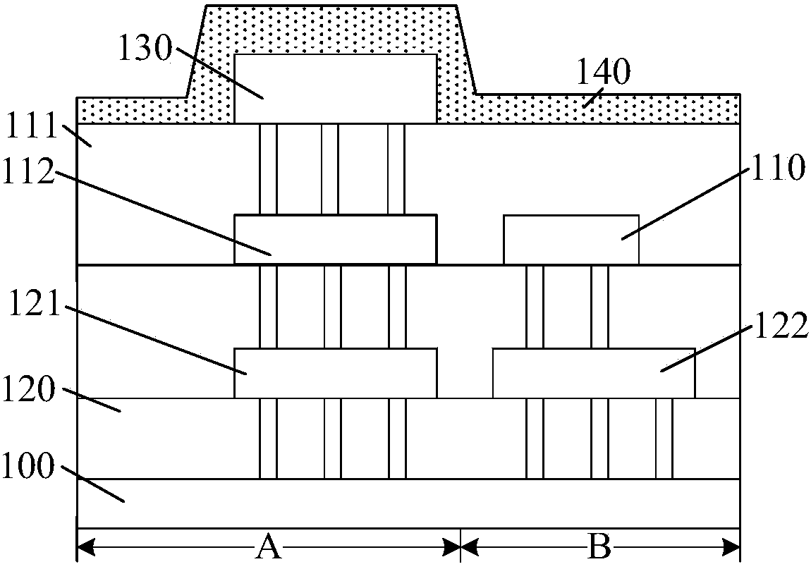
[0037] Figure 1 to Figure 3 It is a structural schematic diagram of each step of a method for forming a fuse device.

[0038] Please refer to figure 1, providing a substrate 100, the substrate 100 includes a logic area A and a fuse area B; an interlayer dielectric structure 120 is formed on the substrate 100 of the logic area A and the fuse area B, and the logic area A interlayer There is an interlayer connection structure 121 in the dielectric structure 120, and a fuse connection structure 122 is provided in the interlayer dielectric structure 120 of the fuse area B; a layer is formed on the interlayer connection structure 121 and the inte...


PUM

PropertyMeasurementUnit
Thicknessaaaaaaaaaa

Abstract

The invention discloses a semiconductor structure and a forming method thereof. The forming method comprises the following steps that a substrate is provided, wherein the substrate comprises a fuse zone; a dielectric structure is formed on the substrate, and a fuse connecting structure is arranged in the fuse zone dielectric structure; a fuse metal layer is formed on the surface of the fuse connecting structure; a stop layer is formed on the fuse metal layer; an initial protection layer is formed on the stop layer; a part of the initial protection layer is etched, and a protection layer is formed, wherein the protection layer exposes the stop layer on the fuse metal layer; and in the etching process, the etching rate of the initial protection layer is larger than that of the stop layer. The stop layer is not easy to be etched and removed, so that the fuse metal layer can be prevented from being exposed. Therefore, the forming method can reduce damage of the fuse metal layer, so that the performance of the formed semiconductor structure can be improved.

Description

technical field [0001] The invention relates to the technical field of semiconductor manufacturing, in particular to a semiconductor structure and a forming method thereof. Background technique [0002] With the development of fuse technology, the application of fuse is becoming more and more extensive. It is not limited to repairing memory cells, but can also be used as a programmable array. [0003] The unit structure of the fuse is mainly provided by several transistors in parallel to provide enough current to blow the fuse, or to blow the fuse by laser irradiation, and to store information by whether the fuse is blown or not. The resistance of the fuse is very small before the fuse is blown, and the resistance increases exponentially after the fuse is blown under the action of a continuous high current, and the state of the fuse blown will remain forever. Therefore, an electric fuse can correspond to "0" and "1" in binary. [0004] In the semiconductor process, fuses o...

Claims


Application Information

Patent Timeline
IPC IPC(8): H01L23/525H01L27/112
CPCH01L23/5256H10B20/20
Inventor 诸俊王亮
Owner SEMICON MFG INT (SHANGHAI) CORP
Features
  • R&D
  • Intellectual Property
  • Life Sciences
  • Materials
  • Tech Scout
  • Unparalleled Data Quality
  • Higher Quality Content
  • 60% Fewer Hallucinations
Learn More