Technology for cutting semiconductor silicon wafer by diamond wire

A diamond wire and semiconductor technology, applied in the field of semiconductor manufacturing, can solve the problems of high cost and low production capacity, and achieve the effect of expanding production capacity, fast cutting speed, and increasing the number of chips produced.

Inactive Publication Date: 2019-03-08
TIANJIN ZHONGHUAN ADVANCED MATERIAL TECH
View PDF5 Cites 3 Cited by
  • Summary
  • Abstract
  • Description
  • Claims
  • Application Information

AI Technical Summary

Problems solved by technology

The cutting of semiconductor silicon wafers adopts the traditional sand wire cutting technology, which has problems such as low production capacity and high cost. There is an urgent need for the development and innovation of diamond wire technology in the semiconductor field.

Method used


Image

  • Technology for cutting semiconductor silicon wafer by diamond wire
  • Technology for cutting semiconductor silicon wafer by diamond wire
  • Technology for cutting semiconductor silicon wafer by diamond wire

Examples


Embodiment Construction

[0035] Unless otherwise defined, the technical terms used in the following embodiments have the same meaning as commonly understood by those skilled in the art to which the present invention belongs. The test reagents used in the following examples, unless otherwise specified, are conventional biochemical reagents; the experimental methods, unless otherwise specified, are conventional methods.

[0036] The present invention will be described in detail below in conjunction with the embodiments and accompanying drawings.

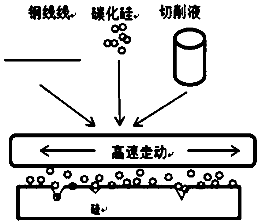
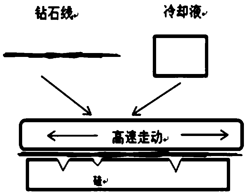
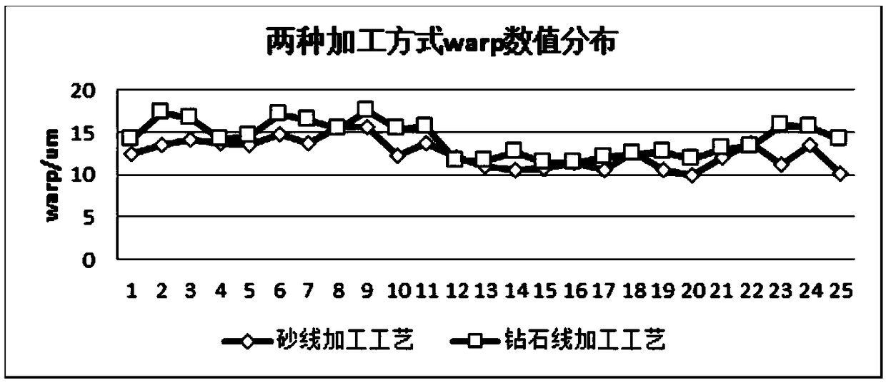
[0037] A process for diamond wire cutting semiconductor silicon wafers, the specific process flow is as follows:

[0038] (1) Take a 6-inch semiconductor silicon single crystal (the single crystal is cylindrical, about 650mm in length, and 150.7mm in diameter) and wipe the surface with absolute ethanol, and take Japanese sticky glue (curing agent A and adhesive The ratio of glue B is 2:1) stick the single crystal to the resin board, and then stick the resin b...


PUM

PropertyMeasurementUnit
warpageaaaaaaaaaa

Abstract

The invention provides a technology for cutting a semiconductor silicon wafer by a diamond wire. Diamond wire equipment is used for cutting the semiconductor silicon wafer, during the cutting process,the falling speed of a worktable is 1.5-2.5 mm / min, the wire speed of diamond wire cutting is 1100-1400m / min, the flow rate of coolant is adjusted to 80-100L / min, the temperature of the coolant is 23-28 DEG C, and the wire supply quantity of steel wire is 0.4-1.5m / sheet. The technology of the diamond wire cutting the semiconductor silicon wafer has the advantages of increasing the number of chipsper kilogram and enlarging the output capacity, and can effectively reduce the costs of existing semiconductor cutting and grinding film and polishing film, and a strong foundation is laid for a large-size polishing film products costs reducing plan.

Description

technical field [0001] The invention belongs to the field of semiconductor manufacturing, and in particular relates to a cutting method of semiconductor silicon wafers, specifically, a diamond wire cutting process for semiconductor silicon wafers. Background technique [0002] According to the "2017 Analysis of my country's Wafer Industry Market Status and Development Trend", due to the high cost of purchasing foreign raw materials by clients at the current stage, the semiconductor industry has initially entered the transition from foreign to domestic purchase plan, and the production capacity of silicon wafers will increase in 2017. Limited, resulting in a supply-demand gap of 3% to 4%; in 2018, it is expected to have a supply-demand gap of about 6%. As a result, the gap between supply and demand transformation continues to expand, and the domestic semiconductor wafer material market has a good development trend. Diamond wire cutting technology has been industrialized in th...

Claims


Application Information

Patent Timeline
Patent Type & Authority Applications(China)
IPC IPC(8): B28D5/04B24B27/06
CPCB24B27/0633B28D5/045
Inventor 常雪岩韩木迪苏晓剑谢艳刘琦武卫
Owner TIANJIN ZHONGHUAN ADVANCED MATERIAL TECH
Why Eureka
Try Eureka