Filter film, preparation method of filter film and electronic control color-changing smart window
A filter film, transparent and conductive technology, applied in optics, nonlinear optics, instruments, etc., can solve the problems of color types of discoloration and difficulty in response speed.
- Summary
- Abstract
- Description
- Claims
- Application Information
AI Technical Summary
Problems solved by technology
Method used
Image
Examples
Embodiment 1
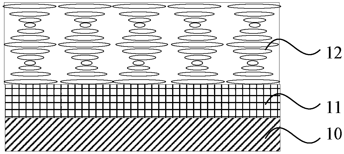
[0044] An embodiment of the present invention provides a filter film, figure 1 For a structural schematic diagram of a filter film provided in an embodiment of the present invention, see figure 1 , the filter film includes: a first conductive transparent substrate 10; a first alignment layer 11 formed on the first conductive transparent substrate 10; a solid polymer liquid crystal 12 formed on the first alignment layer 11, a solid polymer liquid crystal 12 Being a one-dimensional photonic crystal, solid polymer liquid crystal 12 is used to reflect light in a first preselected wavelength range.
[0045] A photonic crystal refers to an artificial periodic dielectric structure with a photonic band gap (Photonic Band-Gap, PBG for short), and is sometimes called a PBG photonic crystal structure.
[0046] An embodiment of the present invention provides a filter film, which includes a solid polymer liquid crystal. The solid polymer liquid crystal 12 is a one-dimensional photonic cry...
Embodiment 2
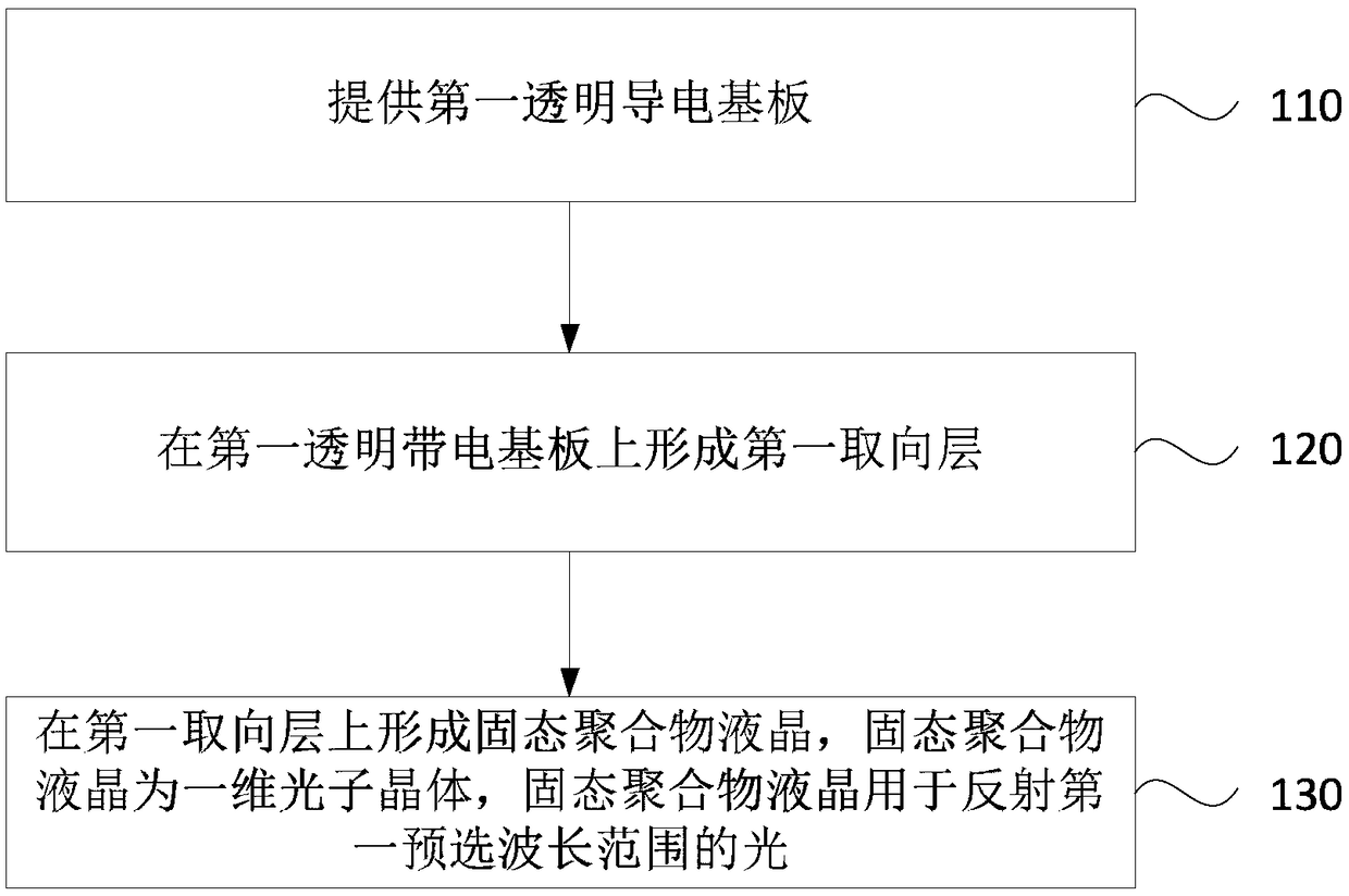
[0066] On the basis of the above-mentioned embodiments, the embodiments of the present invention provide a method for preparing a filter film, figure 2 It is a schematic flowchart of a method for preparing a filter film provided by an embodiment of the present invention. by figure 1 For example, see figure 2 , the method includes the following steps:
[0067] Step 110, providing a first transparent conductive substrate.
[0068] In this embodiment, the first transparent conductive substrate may be transparent indium tin oxide (ITO) glass or polyethylene terephthalate (PET).
[0069] see figure 1 , providing a first transparent conductive substrate 10 .
[0070] Step 120, forming a first alignment layer on the first transparent conductive substrate.
[0071] see figure 1 , forming a first alignment layer 11 on the first transparent conductive substrate 10 .
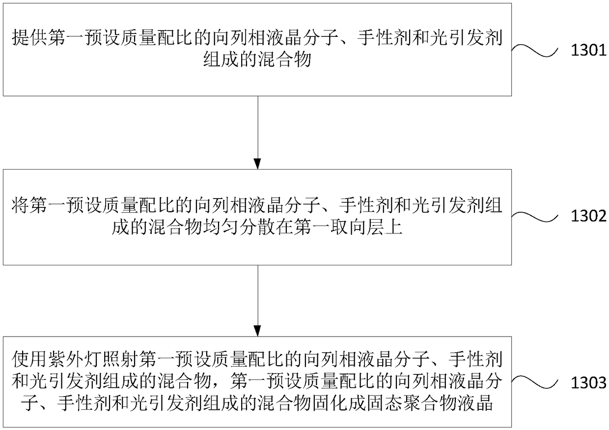
[0072] Specifically, an alignment agent is coated on the first transparent conductive substrate, followed by a...
Embodiment 3
[0086] On the basis of the above-mentioned embodiments, the embodiments of the present invention provide an electronically controlled color-changing smart window. Figure 4 For a schematic structural diagram of an electronically controlled color-changing smart window provided in an embodiment of the present invention, see Figure 4 , the electronically controlled color-changing smart window includes: a second transparent conductive substrate 20, the second transparent conductive substrate 20 includes the light filter film involved in the above embodiment; the second preset mass ratio formed on the second transparent conductive substrate 20 A mixture 30 of a dichroic dye, a dual-frequency liquid crystal, and a second chiral agent, the chiral direction of the second chiral agent is opposite to that of the first chiral agent; The insulating spacer 40 on the mixture 30 of the chromatic dye, the dual-frequency liquid crystal and the second chiral agent; the third transparent conduc...
PUM
| Property | Measurement | Unit |
|---|---|---|
| thickness | aaaaa | aaaaa |
Abstract
Description
Claims
Application Information
 - R&D
- Intellectual Property
- Life Sciences
- Materials
- Tech Scout
- Unparalleled Data Quality
- Higher Quality Content
- 60% Fewer Hallucinations
Browse by: Latest US Patents, China's latest patents, Technical Efficacy Thesaurus, Application Domain, Technology Topic, Popular Technical Reports.
© 2025 PatSnap. All rights reserved.Legal|Privacy policy|Modern Slavery Act Transparency Statement|Sitemap|About US| Contact US: help@patsnap.com


