Flexible single crystal Lamb wave resonator and method of forming same

A single crystal Lamb wave resonator, flexible technology, applied in the direction of impedance network, electrical components, etc., can solve the problems of reduced device performance, device scrapping, unevenness, and achieve the effect of improving the success rate of transfer

Active Publication Date: 2022-03-18
TIANJIN UNIV
View PDF6 Cites 0 Cited by
  • Summary
  • Abstract
  • Description
  • Claims
  • Application Information

AI Technical Summary

Problems solved by technology

In addition, the crystal ion slicing technology cannot control the stress, so that the prepared single crystal thin film has residual stress. After the cavity release process, the residual stress will cause the single crystal thin film to bend or crack to reduce the performance of the device, or even directly break and cause the device scrapped
Finally, during the process of dry etching the top of the silicon substrate, due to the isotropy of dry etching, the bottom of the released cavity will be uneven, which will easily lead to device damage during subsequent transfer.

Method used


Image

  • Flexible single crystal Lamb wave resonator and method of forming same
  • Flexible single crystal Lamb wave resonator and method of forming same
  • Flexible single crystal Lamb wave resonator and method of forming same

Examples


Embodiment 1

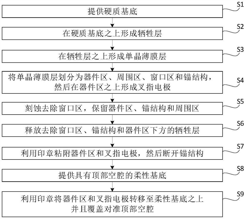
[0055] The hard substrate 101 having a silicon material having a thickness of about 400 μm is provided, and a sacrificial layer 102 having a thickness of from 0.1 to 10 μm (preferably 1 μm) is formed over the hard substrate 101 by a chemical vapor deposition process, and then by ion The slice process is a single crystal thin film layer 103 of a lithium niobic acid lithium niobate material having a thickness of 0.1 to 2 μm (preferably 0.7 μm) above the sacrificial layer 102.

[0056] It is to be explained that the ion slicing process specifically refers to the front injection of the lithium niobate wafer + Ion, make HE + Ions are injected into a certain depth of the lithium niobate wafer and form a HE + Ion layer, then by heating annealing process makes he + The HE molecule bubbles are formed, thereby peeling the film layer. Finally, the lithium niobate film layer was thinned to a designated thickness of 0.1 to 2 μm to 0.7 μm using a chemical mechanical polishing (CMP) process. The...

Embodiment 2

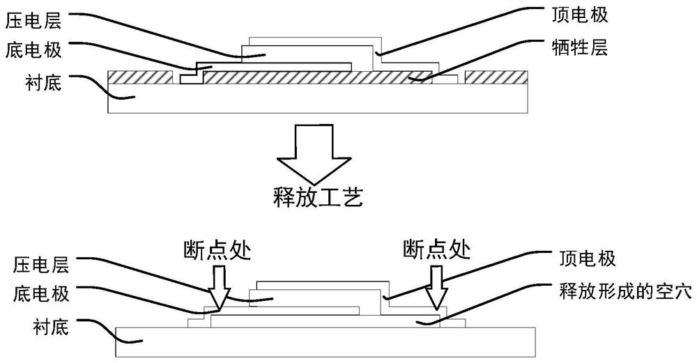
[0068] First, the next order is formed in order Figure 14 The four-layer structure shown, including a hard base layer 101, a sacrificial layer 102, a metal layer 107 (thickness of about 0.1 μm), and a single crystal film layer 103. Then, a single crystal film region division, etching window, and release cavity will be performed in the steps in Example 1. The release process removal of the device structure after the silica of the sacrificial layer 102 is Figure 15 As shown, the bottom electrode 107 'is formed below the device area 103a. Continue with reference to the step of the step in Example 1, the resonator structure is transferred from the hard substrate to the flexible substrate with top cavities. The final device is like Figure 16 Indicated.


PUM

PropertyMeasurementUnit
thicknessaaaaaaaaaa
thicknessaaaaaaaaaa
thicknessaaaaaaaaaa

Abstract

The invention provides a flexible single crystal Lamb wave resonator and a forming method thereof. The method includes: providing a hard substrate; forming a sacrificial layer on the hard substrate; forming a single crystal thin film layer on the sacrificial layer; dividing the single crystal thin film layer into a device area, a peripheral area, a window area and an anchor structure, the window The area is used to separate the device area from the surrounding area, the anchor structure is used to connect the device area and the surrounding area, and then an interdigital electrode is formed on the device area; the window area is removed by etching, and the device area, the anchor structure and the surrounding area are retained; Release and remove the sacrificial layer under the window region, anchor structure and device region, so that the device region and interdigital electrodes are suspended on the hard substrate under the action of the anchor structure; use a stamp to adhere the device region and interdigital electrodes, and then disconnect Anchor structure to detach the device region and interdigital electrodes from the rigid substrate; provide a flexible substrate with a top cavity; transfer the device region and interdigital electrodes onto the flexible substrate and cover align the top cavity using a stamp.

Description

Technical field [0001] The present invention relates to the field of semiconductors, and in particular, to a flexible single crystal rum wave resonator and a forming method thereof. Background technique [0002] Including the new application of the Internet of Things and 5G, a higher requirement for the power consumption and bandwidth of the resonator, and the Lamobo resonator having a single crystal material such as lithium niobate and lithium tantalum is highly KT2. And the high Q value, which can meet the requirements of the next generation of reconstructed and multi-band wideband filtering. Ultra-lowEwake-upRecivers is also a major research hotspot for single crystal Lanmo resonators. The traditional Lambo resonators are based on a hard substrate, which makes the demand for flexible electronic fields (such as flexible resonators, filters, oscillators, sensors) still cannot meet, so it is urgent to develop a flexible Rumbo Resonator. [0003] The existing method of preparing f...

Claims


Application Information

Patent Timeline
Patent Type & Authority Patents(China)
IPC IPC(8): H03H9/02H03H9/17
CPCH03H9/02039H03H9/02086H03H9/171
Inventor 庞慰孙新张孟伦
Owner TIANJIN UNIV
Why Eureka
Try Eureka