Capacitor structure and manufacturing method thereof
A capacitor structure and manufacturing method technology, which is applied in semiconductor/solid-state device manufacturing, circuits, electrical components, etc., can solve problems such as limited amplitude, increased electric field strength, and high and low fluctuations in the shape of the process, so as to increase the effective area. , Improve capacitance density, reduce production cost
- Summary
- Abstract
- Description
- Claims
- Application Information
AI Technical Summary
Problems solved by technology
Method used
Image

Examples
Embodiment 1
[0043] image 3 It is a flow chart of a manufacturing method of a capacitor structure provided in this embodiment, such as image 3 As shown, the present invention provides a method for manufacturing a capacitor structure, comprising the following steps:
[0044] S01: providing a substrate;
[0045] S02: Etching the substrate to form a plurality of grooves, using the remaining substrate as a plate of the capacitor;
[0046] S03: forming a capacitor dielectric layer on the inner wall of the trench;
[0047] S04: Form a conductive layer in the trench, and use the conductive layer as another polar plate of the capacitor.
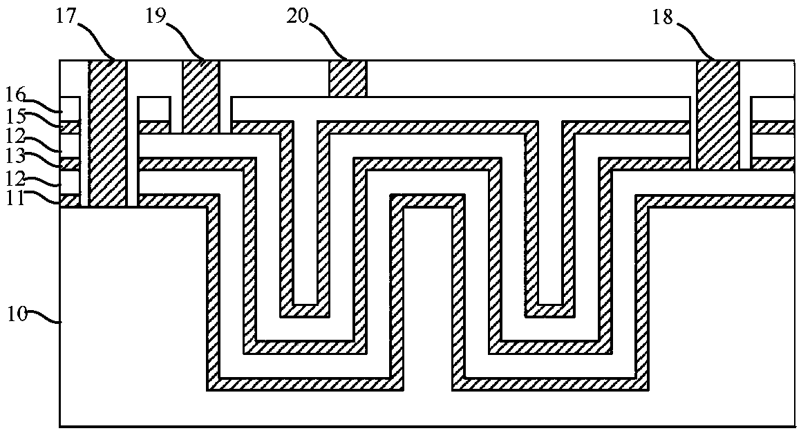
[0048] Figure 4a-Figure 4c It is a structural diagram corresponding to the relevant steps in the manufacturing process of a capacitor structure provided in this embodiment, please refer to image 3 and combine Figure 4a-Figure 4c , to describe in detail the fabrication method of a capacitor structure provided by this embodiment.
[0049] Step S01 is pe...
Embodiment 2
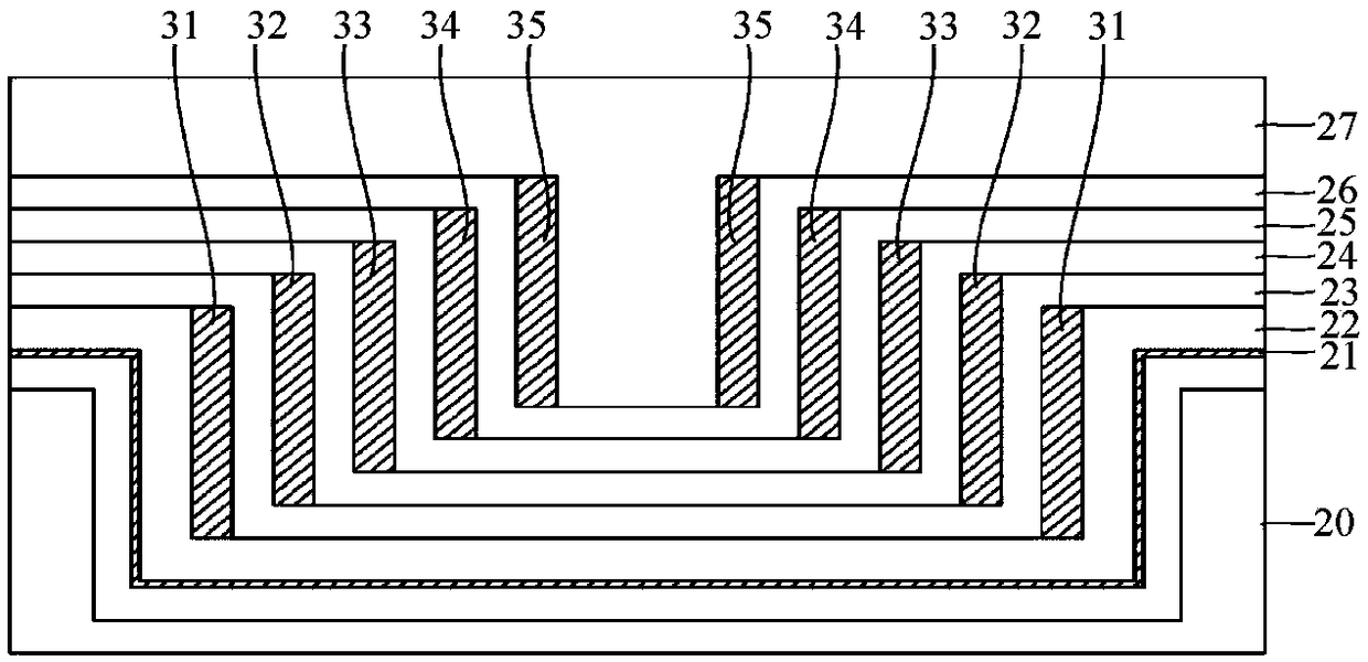
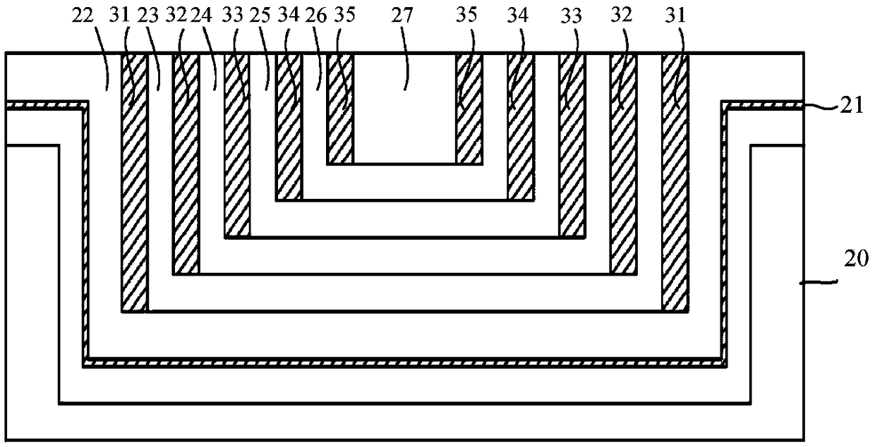
[0059] Figure 5 is a flow chart of a manufacturing method of a capacitor structure provided in this embodiment, Figure 6a-6d It is a structural schematic diagram corresponding to relevant steps in the manufacturing process of a capacitor structure provided in this embodiment. Please refer to Figure 5 and combine Figure 6a-6d , the present embodiment provides another method for manufacturing a capacitor structure, including:
[0060] Step S11: providing a substrate, and etching the substrate to form grooves;
[0061] Step S12: depositing a polysilicon layer in the groove;
[0062] Step S13: Etching the polysilicon to form several trenches, using the remaining polysilicon as the first plate of the capacitor;
[0063] Step S14: forming a capacitor dielectric layer on the inner wall of the trench;
[0064] Step S15 : forming a conductive layer in the trench, using the conductive layer as a second plate of the capacitor.
[0065] Specifically, firstly, a substrate 200 is...
PUM
 Abstract
Description
Claims
Application Information
 - R&D
- Intellectual Property
- Life Sciences
- Materials
- Tech Scout
- Unparalleled Data Quality
- Higher Quality Content
- 60% Fewer Hallucinations
Browse by: Latest US Patents, China's latest patents, Technical Efficacy Thesaurus, Application Domain, Technology Topic, Popular Technical Reports.
© 2025 PatSnap. All rights reserved.Legal|Privacy policy|Modern Slavery Act Transparency Statement|Sitemap|About US| Contact US: help@patsnap.com