
Preparation method and tooling of photoresist microstructure of large-aperture thin-film diffractive lens

A technology of diffractive lens and photoresist, which is applied in microlithography exposure equipment, photoplate making process of patterned surface, optomechanical equipment, etc. It can solve the problems that imaging cannot be realized, and it is difficult to obtain wave aberration that meets imaging requirements. , to achieve the effect of high-resolution optical imaging

Active Publication Date: 2020-10-16
INST OF OPTICS & ELECTRONICS - CHINESE ACAD OF SCI
View PDF13 Cites 0 Cited by
  • Summary
  • Abstract
  • Description
  • Claims
  • Application Information

AI Technical Summary

Problems solved by technology

This method largely takes advantage of the advantages of traditional microfabrication technology, but for thin film diffractive lenses, the thin film substrate with microstructure is very sensitive to the horizontal deformation in the mirror surface, and the cast film forming method separates the thin film from the substrate. When , it is very easy to cause lateral stress release or in-plane deformation, so it is difficult to obtain wave aberration that meets the imaging requirements
Even if high diffraction efficiency can be obtained, good imaging cannot be achieved

Method used


Image

  • Preparation method and tooling of photoresist microstructure of large-aperture thin-film diffractive lens
  • Preparation method and tooling of photoresist microstructure of large-aperture thin-film diffractive lens

Examples


Embodiment Construction

[0031] The present invention will be described in detail below in conjunction with the accompanying drawings and specific embodiments.

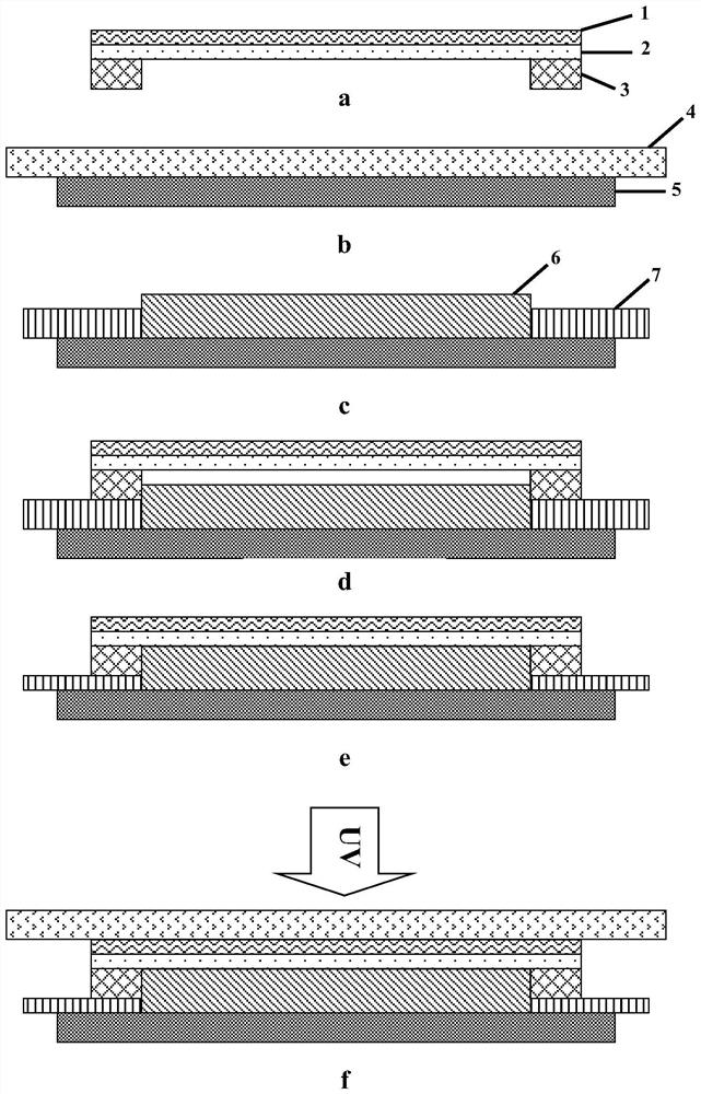
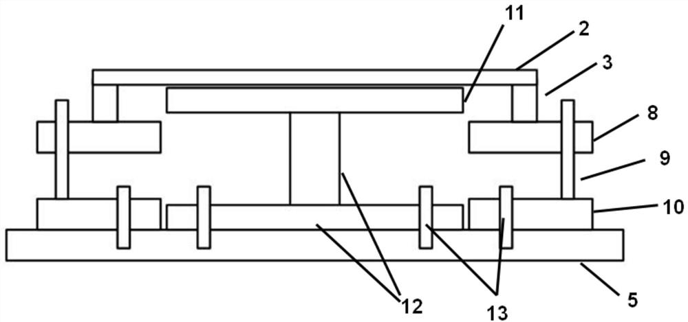
[0032] The present invention takes the preparation of photoresist microstructure of polyimide film diffractive lens with 400 mm aperture as an example, combined with the schematic diagram of the preparation method of photoresist microstructure of large aperture film diffractive lens figure 1 of figure 1 a- figure 1 f, The principle and process steps of the preparation method of the photoresist microstructure of the large-aperture thin-film diffractive lens in detail. in, figure 1 a is a schematic diagram of the coating process steps of the method for preparing the photoresist microstructure of the large-aperture thin-film diffractive lens; figure 1 b is a schematic diagram of the datum plane leveling process steps of the method for preparing the photoresist microstructure of the large-aperture thin film diffractive lens; figure 1 c is a s...


PUM

PropertyMeasurementUnit
surface smoothnessaaaaaaaaaa
thicknessaaaaaaaaaa

Abstract

The invention discloses a preparation method and device for a photoresist microstructure of a large-aperture thin film diffraction lens, and solves the problem that the same high-quality photoresist microstructures can not be obtained in different radius regions when a traditional approach / contact exposure method is used for preparing the large-aperture thin film diffraction lens. According to theprovided preparation method for the photoresist microstructure of the large-aperture thin film diffraction lens, the large-aperture thin film diffraction lens with large-area and high-quality photoresist shapes on the surface is prepared without affecting the wavefront aberration of the large-aperture thin film diffraction lens. The method can stably control wavefront distortion fluctuation caused by the photoresist exposure process of the large-aperture thin film diffraction lens, the uniformity of full-aperture exposure gaps is high, the full-aperture photoresist shapes are excellent, the exposure process conditions are stable and easily controlled, repeatability is good, toxics and harm are avoided, and popularization is facilitated.

Description

technical field [0001] The invention belongs to the field of microstructure manufacturing of diffractive optical elements, and in particular relates to a method for preparing a photoresist microstructure of a large-aperture film diffractive lens and a tooling. Background technique [0002] Large-aperture space telescopes are widely used in astronomy, aviation, aerospace, military and civilian fields, especially the development of modern warfare has put forward higher requirements for space remote sensing systems. Earth remote sensing satellites have the advantages of high timeliness and continuous detection capabilities, which are suitable for the needs of future military development. [0003] In order to further obtain high-quality and high-resolution observation images of farther targets and improve the resolution of earth remote sensing satellites, a larger aperture is the most basic requirement. However, the existing traditional large-aperture telescopes are limited by ...

Claims


Application Information

Patent Timeline
Patent Type & Authority Patents(China)
IPC IPC(8): G02B27/42G03F7/20
CPCG02B27/4233G03F7/70716G03F7/70733
Inventor 李志炜邵俊铭蒋青锋高国涵汪利华石恒雷柏平罗倩刘盾范斌
Owner INST OF OPTICS & ELECTRONICS - CHINESE ACAD OF SCI
Learn More