
A large-aperture film diffractive lens microstructure etching transfer method and tooling

A diffractive lens and microstructure technology, applied in optical elements, instruments, optics, etc., can solve the problems of etching environment change, full-chip etching non-uniformity, and no large-diameter thin-film diffractive lens etching transfer process, etc. High resolution optical imaging, high diffraction efficiency uniformity effect

Active Publication Date: 2020-10-16
INST OF OPTICS & ELECTRONICS - CHINESE ACAD OF SCI
View PDF9 Cites 0 Cited by
  • Summary
  • Abstract
  • Description
  • Claims
  • Application Information

AI Technical Summary

Problems solved by technology

However, reactive ion etching has not been directly used in the microstructure transfer process and production of large-aperture thin-film diffractive lenses. One of the reasons is that there are few commercial reactive ion etching equipment with an aperture larger than 400 mm, which can be used for 450 mm in semiconductor production. Millimeter reactive ion etching equipment is being developed, so there is no available large-diameter thin film diffraction lens etching transfer process; secondly, the reactive ion etching process is an extremely complex comprehensive process of chemical and physical reactions, radio frequency electric field, chamber The structure, substrate material, etc. can seriously affect the etching results, so it is difficult to obtain a simulation model or semi-empirical formula with strong experimental guiding significance like the physical bombardment etching model. It causes a large change in the etching environment, so that the existing process parameters cannot be directly applied to the microstructure transfer of large-aperture thin-film diffractive imaging lenses
The traditional reactive ion etching process is either aimed at silicon wafers of about 1 mm, or is suitable for small-caliber quartz substrates that do not require too much thickness to maintain the surface shape. For the frame that must be more than 20 mm thick to maintain the surface shape, and the central area of ​​​​the film must be suspended Light-transmitting large-aperture thin-film diffractive lens, the traditional reactive ion etching method cannot obtain the etching transfer effect similar to the high etching rate and high etching uniformity in the production of small-aperture binary optical elements
In our previous experiments, the etching transfer rate of the 400 mm aperture thin film diffractive lens using the traditional process is only one-third of that of the small aperture binary optical element, and the etching non-uniformity of the whole chip exceeds ±20%.

Method used


Image

  • A large-aperture film diffractive lens microstructure etching transfer method and tooling
  • A large-aperture film diffractive lens microstructure etching transfer method and tooling

Examples


Embodiment Construction

[0031] The present invention will be described in detail below in conjunction with the accompanying drawings.

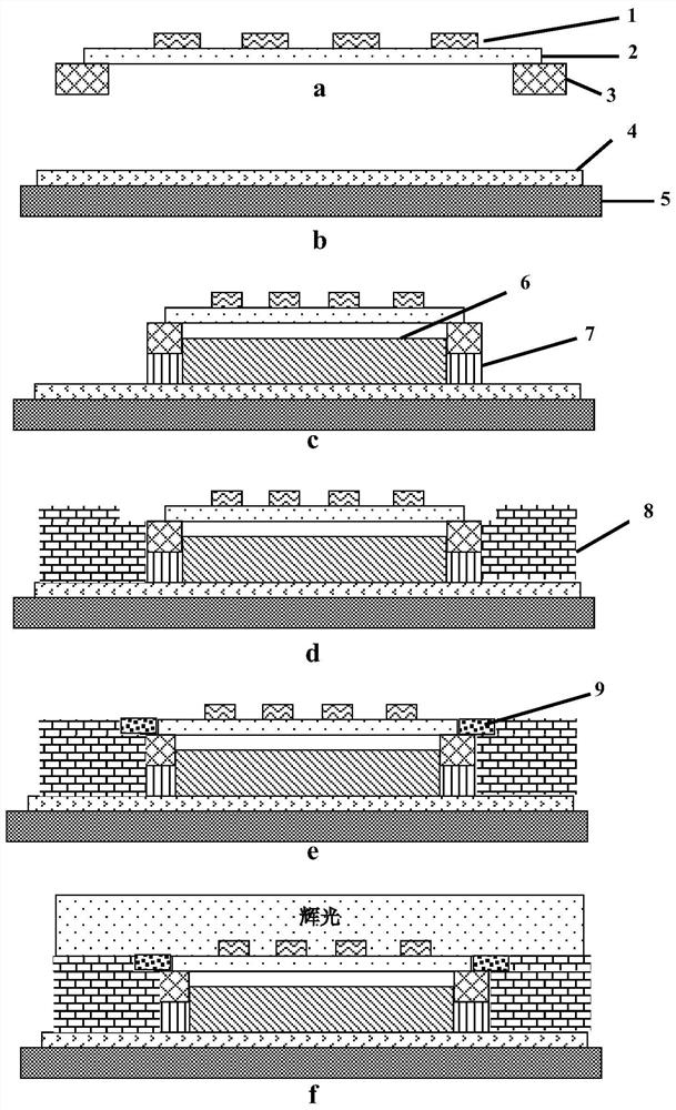
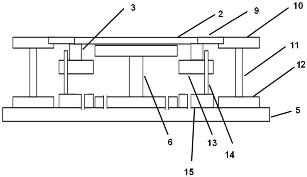
[0032] The present invention takes 400 mm diameter polyimide film diffractive lens microstructure reactive ion etching transfer as an example, combined with large aperture thin film diffractive lens microstructure reactive ion etching transfer method schematically figure 1 of figure 1 a- figure 1 f, The principle and process steps of the reactive ion etching transfer method for the microstructure of the large-aperture thin-film diffractive lens in detail. in, figure 1 a is a schematic diagram of the process steps for preparing etching samples by the etching transfer method of the microstructure of the large-aperture thin-film diffractive lens; figure 1 b is a schematic diagram of the graphite felt matting process steps of the large-aperture thin film diffractive lens microstructure etching transfer method; figure 1 c is a schematic diagram of the filling tooling ...


PUM

PropertyMeasurementUnit
radiusaaaaaaaaaa
depthaaaaaaaaaa
diameteraaaaaaaaaa

Abstract

The invention relates to an etching transfer method and tool for a microstructure of a large-aperture thin film diffraction lens and solves the problem that the large-aperture thin film diffraction lens can not uniformly transfer a photoresist microstructure to a film substrate through reactive ion etching. According to the provided etching transfer method and tool for the microstructure of the large-aperture thin film diffraction lens, the whole high-uniformity micro-structure etching transfer can be achieved in a traditional single-frequency capacitive coupled large-aperture reactive ion etching equipment, the uniformity requirement of the imaging diffraction efficiency of the large-aperture thin film diffraction lens is met, it can be ensured that the wavefront distortion of the large-aperture thin film diffraction lens does not change much with the microstructure etching transfer process before and after etching, and the uniformity of the whole aperture etching depth is better than+ / -6%. The etching process conditions are stable and easy to control, the repeatability is good, the method can be adapted to various types of thin film frames, operation is convenient, and popularization is facilitated.

Description

technical field [0001] The invention designs a large-diameter thin-film diffractive lens microstructure transfer method and tooling, and belongs to the field of diffractive optical element microstructure manufacture. Background technique [0002] Large-aperture space telescopes are widely used in astronomy, aviation, aerospace, military and civilian fields, especially the development of modern warfare has put forward higher requirements for space remote sensing systems. Earth remote sensing satellites have the advantages of high timeliness and continuous detection capabilities, which are suitable for the needs of future military development. [0003] In order to further obtain high-quality and high-resolution observation images of farther targets and improve the resolution of earth remote sensing satellites, a larger aperture is the most basic requirement. However, the existing traditional large-aperture telescopes are limited by the surface mass density of traditional mirr...

Claims


Application Information

Patent Timeline
Patent Type & Authority Patents(China)
IPC IPC(8): G02B27/42
CPCG02B27/4233
Inventor 李志炜邵俊铭巩畅畅蒋青峰高国涵汪利华石恒雷柏平边疆范斌
Owner INST OF OPTICS & ELECTRONICS - CHINESE ACAD OF SCI
Learn More