Method for establishing auxiliary graph exposure model

A technology that assists patterns and models. It is applied in the photoengraving process of the pattern surface, the originals for opto-mechanical processing, optics, etc. It can solve the defects of silicon wafers, poor photoresist conformality, and affect device performance or yield. and other problems to achieve high accuracy

Pending Publication Date: 2019-03-19
上海微阱电子科技有限公司
View PDF4 Cites 5 Cited by
  • Summary
  • Abstract
  • Description
  • Claims
  • Application Information

AI Technical Summary

Problems solved by technology

For example, the auxiliary pattern is imaged on the silicon wafer (AF print); the small-sized photoresist has poor conformality and may easily cause photoresist peeling to introduce defects on the silicon wafer, etc.
These will form unnecessary graphics on the main graphics, affecting device performance or yield

Method used


Image

  • Method for establishing auxiliary graph exposure model
  • Method for establishing auxiliary graph exposure model
  • Method for establishing auxiliary graph exposure model

Examples


Embodiment Construction

[0039] The specific embodiment of the present invention will be further described in detail below in conjunction with the accompanying drawings.

[0040] It should be noted that, in the following specific embodiments, when describing the embodiments of the present invention in detail, in order to clearly show the structure of the present invention for the convenience of description, the structures in the drawings are not drawn according to the general scale, and are drawn Partial magnification, deformation and simplification are included, therefore, it should be avoided to be interpreted as a limitation of the present invention.

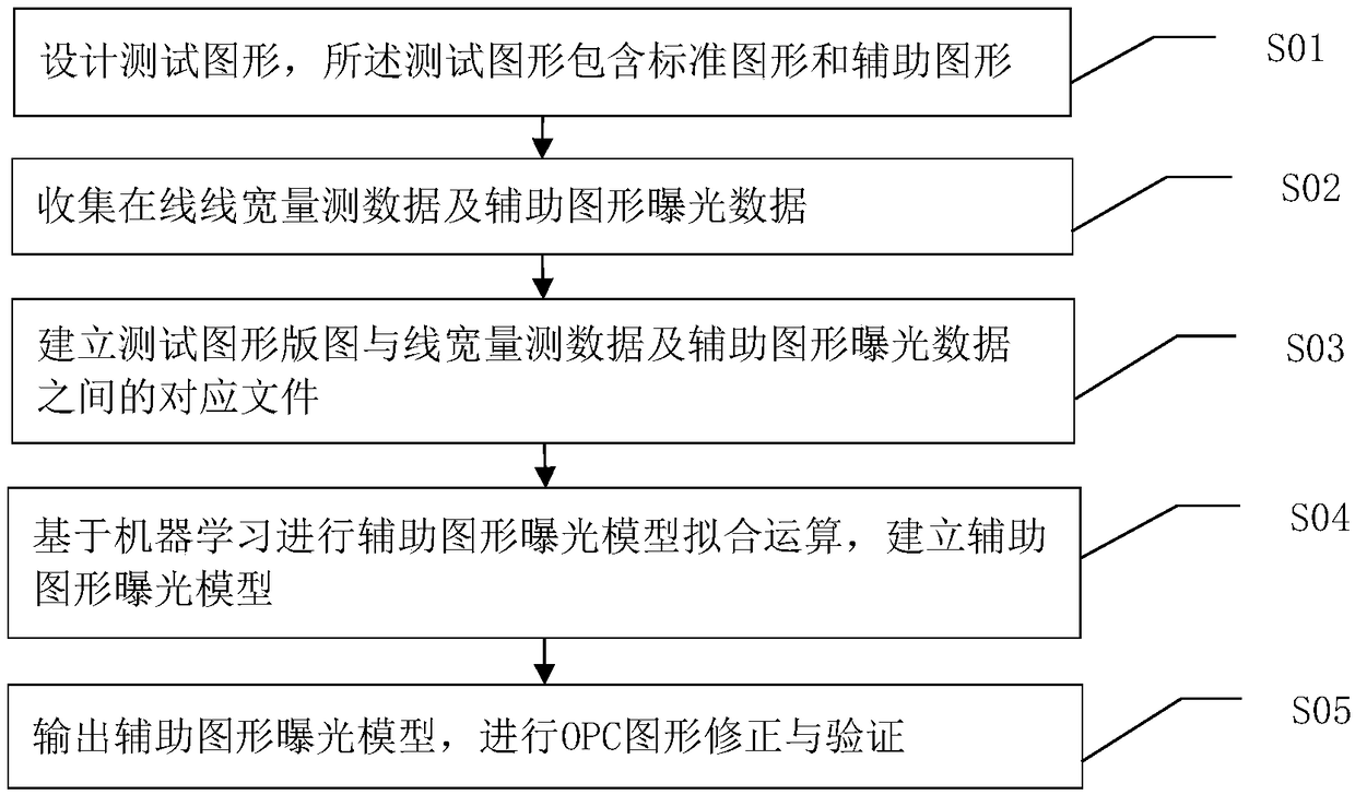
[0041] In the following specific embodiments of the present invention, please refer to figure 1 , figure 1 It is a flowchart of a method for establishing an auxiliary graphic exposure model in the present invention. Such as figure 1 As shown, a method of establishing an auxiliary graphic exposure model of the present invention comprises the follow...


PUM


Abstract

The invention discloses a method for establishing an auxiliary graph exposure model. The method comprises the following steps: S01, designing a test graph, including standard graphs and auxiliary graphs; S02, collecting online line width measurement data and auxiliary graph exposure data; S03, establishing a testing graph layout and a corresponding file between the line width measurement data andthe auxiliary graph exposure data; S04, performing auxiliary graph exposure model fitting operation based on machine learning to establish an auxiliary graph exposure model; and S05, outputting the auxiliary graph exposure model, and performing OPC graph correction and verification. By adopting the method, an auxiliary graph exposure model with higher accuracy can be obtained.

Description

technical field [0001] The invention relates to the technical field of optical proximity effect correction, and more specifically, to a method for establishing an auxiliary graphic exposure model based on machine learning. Background technique [0002] With the continuous development of integrated circuits and the continuous development of manufacturing technology towards smaller dimensions, the photolithography process has become the main bottleneck restricting the development of integrated circuits to smaller feature sizes. In deep sub-micron semiconductor manufacturing, the size of the key pattern is much smaller than the wavelength of the light source. Due to the diffraction effect of light, the pattern projected on the silicon wafer by the mask will change greatly, such as the change of line width and the corner Various optical proximity effects such as the rounding of the wire and the shortening of the line length. In order to compensate for the influence of these eff...

Claims


Application Information

Patent Timeline
Patent Type & Authority Applications(China)
IPC IPC(8): G03F1/36
CPCG03F1/36
Inventor 卢意飞
Owner 上海微阱电子科技有限公司
Why Eureka
Try Eureka