Unlock instant, AI-driven research and patent intelligence for your innovation.

Conductive pattern and manufacturing method thereof, display substrate, display device

A technology of conductive graphics and production methods, which is applied in semiconductor/solid-state device manufacturing, circuits, electrical components, etc., and can solve problems such as increased bending of substrates, equipment alarms, broken substrates, etc.

Active Publication Date: 2021-03-19
BOE TECH GRP CO LTD
View PDF4 Cites 0 Cited by
  • Summary
  • Abstract
  • Description
  • Claims
  • Application Information

AI Technical Summary

Problems solved by technology

[0003] However, when the Cu thin film is formed on the base substrate by sputtering process, a large stress will be generated. As the sputtering thickness increases, the stress will also increase, resulting in a larger bending degree of the base substrate; this bending will Cause equipment alarm or substrate substrate breakage, affecting the performance and product yield of the display substrate

Method used


Image

  • Conductive pattern and manufacturing method thereof, display substrate, display device
  • Conductive pattern and manufacturing method thereof, display substrate, display device
  • Conductive pattern and manufacturing method thereof, display substrate, display device

Examples


Embodiment Construction

[0039] In order to make the technical problems, technical solutions and advantages to be solved by the embodiments of the present invention clearer, the following will describe in detail with reference to the drawings and specific embodiments.

[0040] Embodiments of the present invention provide a conductive pattern and a manufacturing method thereof, a display substrate, and a display device, which can improve the product yield of the display substrate while realizing a low-resistance conductive pattern.

[0041] Embodiments of the present invention provide a method for making a conductive pattern, including:

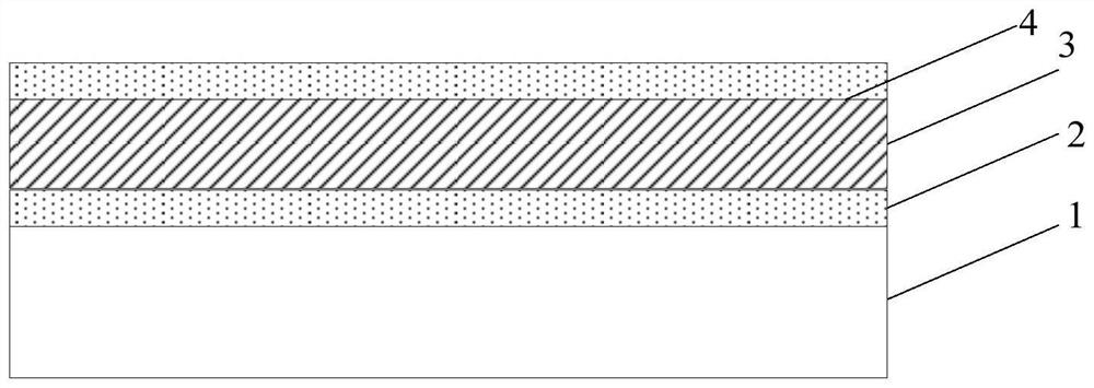
[0042] Step 1, forming a metal layer on the base substrate;

[0043] Step 2, forming a conductive buffer layer on the metal layer;

[0044] Step 3, patterning the metal layer and the conductive buffer layer to form a sub-conductive pattern;

[0045] Repeat the above steps 1-3 to form a plurality of sub-conductive patterns arranged in layers. The plurality of sub-con...


PUM

PropertyMeasurementUnit
thicknessaaaaaaaaaa

Abstract

The invention provides a conductive pattern and a manufacturing method thereof, a display substrate and a display device, belonging to the field of display technology. Wherein, the method for making the conductive pattern comprises: step 1, forming a metal layer on the base substrate; step 2, forming a conductive buffer layer on the metal layer; step 3, performing a process on the metal layer and the conductive buffer layer Composition to form a sub-conductive pattern; repeat the above steps 1-3 to form a plurality of sub-conductive patterns stacked, the plurality of sub-conductive patterns form the conductive pattern, and the formed sub-conductive pattern is on the positive side of the substrate substrate. The projection falls within the orthographic projection of the previously formed sub-conductive pattern on the base substrate. The technical solution of the invention can improve the product yield of the display substrate while realizing the low-resistance conductive pattern.

Description

technical field [0001] The invention relates to the field of display technology, in particular to a conductive pattern and a manufacturing method thereof, a display substrate, and a display device. Background technique [0002] With the increasing size of LCD (liquid crystal display) and OLED (organic electroluminescent diode) products, higher refresh frequency, higher resolution and higher aperture ratio, there is a demand for low-resistance thick Cu wire technology growing stronger. [0003] However, when the Cu thin film is formed on the base substrate by sputtering process, a large stress will be generated, and as the sputtering thickness increases, the stress will also increase, resulting in greater bending of the base substrate; this bending will It will cause the equipment to alarm or the substrate substrate to be broken, which will affect the performance and product yield of the display substrate. Contents of the invention [0004] The technical problem to be sol...

Claims


Application Information

Patent Timeline
Patent Type & Authority Patents(China)
IPC IPC(8): H01L21/3213H01L23/49H01L29/423
CPCH01L21/32139H01L23/49H01L29/42376H01L21/2855H01L21/76885H01L23/53238H01L27/1244H01L27/1288H01L29/45H01L29/458H01L29/4908C23C14/025C23C14/042C23C14/18C23C14/5873H01L23/562H01L27/124H01L29/401
Inventor 汪建国曹占锋李海旭
Owner BOE TECH GRP CO LTD