A silicon-based optical antenna and its preparation method

An optical antenna and grating technology, applied in the field of antennas, can solve the problems of serious light divergence, low radiation efficiency, and large grating lobe energy, and achieve a small far-field divergence angle, high radar scanning resolution, and high grating lobe suppression effect. Effect

Active Publication Date: 2020-06-23
BEIJING WANJI TECH
View PDF7 Cites 0 Cited by
  • Summary
  • Abstract
  • Description
  • Claims
  • Application Information

AI Technical Summary

Problems solved by technology

[0004] The embodiment of the present invention provides a silicon-based optical antenna, which is used to solve the problems in the prior art that the grating-type optical antenna has serious light divergence, extremely low radiation efficiency, and the energy of the grating lobes after interference is relatively large, which is not well suppressed.

Method used


Image

  • A silicon-based optical antenna and its preparation method
  • A silicon-based optical antenna and its preparation method
  • A silicon-based optical antenna and its preparation method

Examples


preparation example Construction

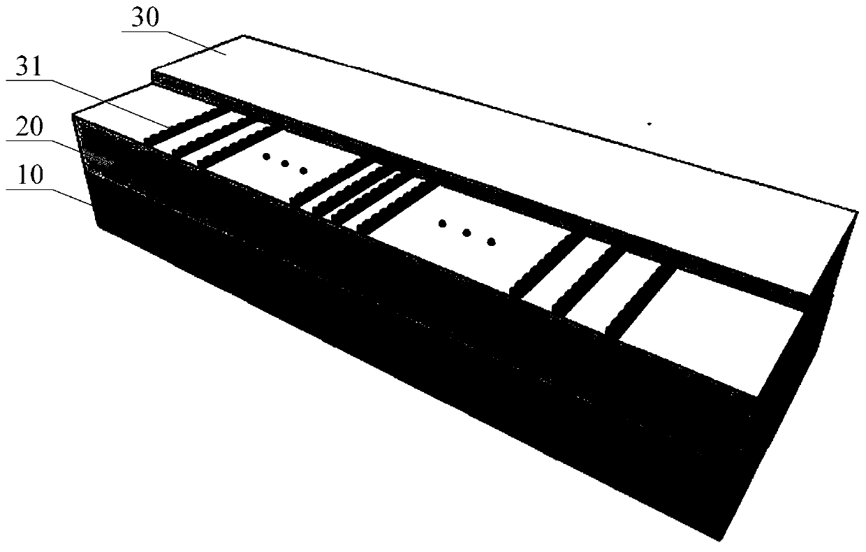
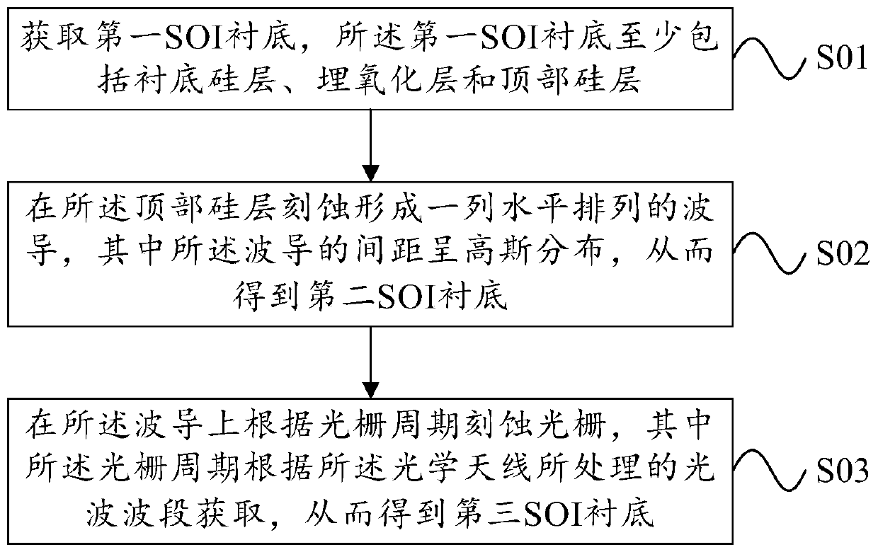
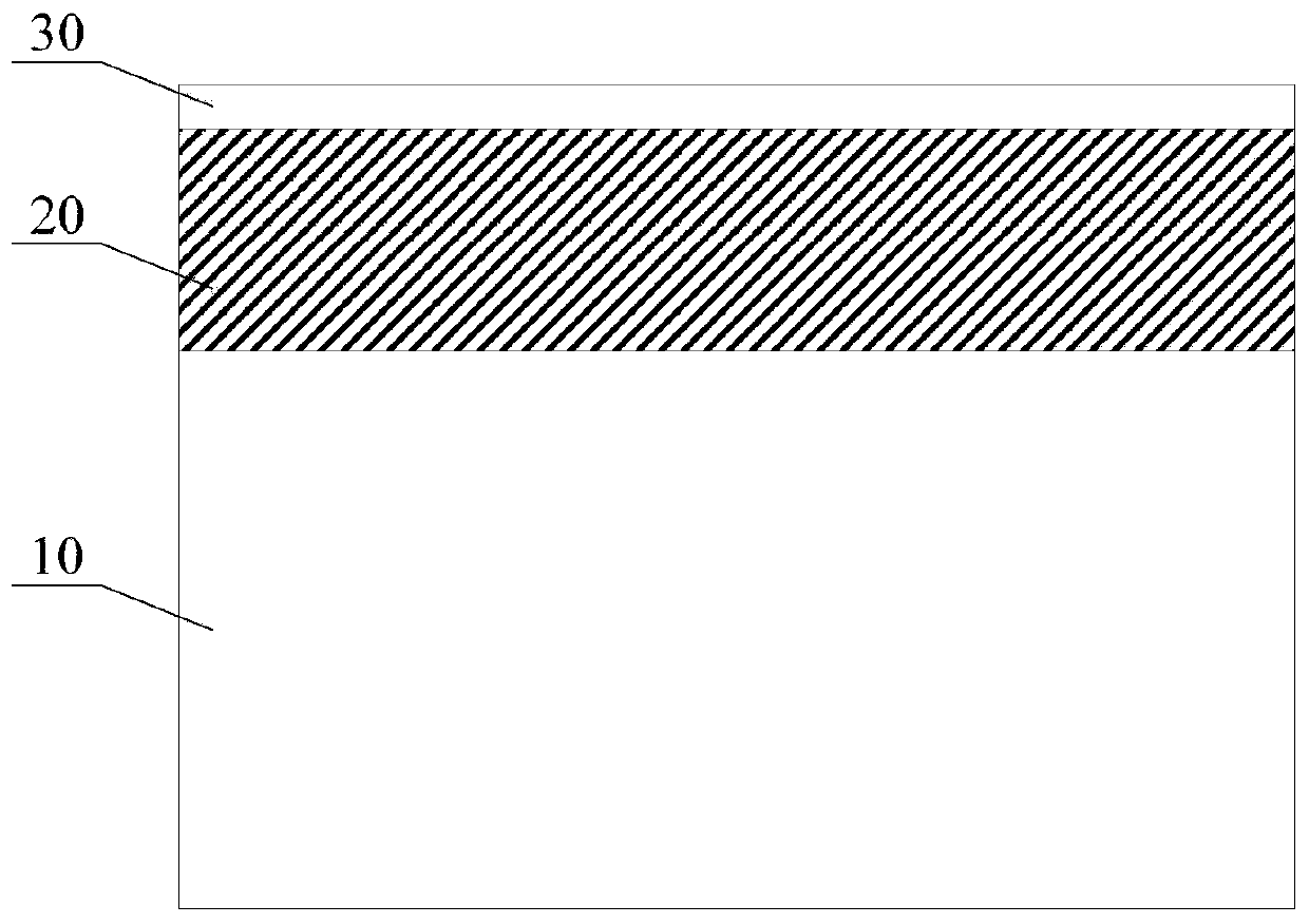
[0034] figure 2 It is a schematic flow chart of a method for preparing a silicon-based optical antenna according to an embodiment of the present invention, image 3 It is a schematic diagram of the structure of the first SOI substrate according to the embodiment of the present invention, Figure 4 It is a schematic diagram of the structure of the second SOI substrate according to the embodiment of the present invention, Figure 5 It is a schematic diagram of the structure of the third SOI substrate according to the embodiment of the present invention, such as figure 2 As shown, the method includes:

[0035] Step S01, obtaining a first SOI substrate, the first SOI substrate at least includes a substrate silicon layer 10, a buried oxide layer 20 and a top silicon layer 30;


PUM

PropertyMeasurementUnit
thicknessaaaaaaaaaa
thicknessaaaaaaaaaa
thicknessaaaaaaaaaa

Abstract

The invention provides a silicon-based optical antenna and a preparation method. The silicon-based optical antenna comprises an SOI substrate, the SOI substrate at least comprises a substrate siliconlayer, a buried oxidation layer and a top silicon layer, the buried oxidation layer is positioned between the substrate silicon layer and the top silicon layer, the top silicon layer of the SOI substrate is etched to form a row of waveguides arranged horizontally, the spacing of the waveguides is in Gaussian distribution, and each waveguide is engraved with a grating. A waveguide array in the optical antenna is arranged in Gaussian distribution, so that light waves can realize a low far-field divergence angle, a good grating lobe inhibition effect, and high horizontal and vertical radar scanning resolution when passing a 2D diffraction grating.

Description

technical field [0001] Embodiments of the present invention relate to the technical field of antennas, in particular to a silicon-based optical antenna and a preparation method thereof. Background technique [0002] The concept of phased array lidar has been proposed long ago, and various design schemes are constantly being developed, and its basic modules are also mature, such as light source, beam splitting, modulation, etc., but how to phase-modulate the light of each waveguide Efficiently exporting photonic integrated circuits remains a great challenge. This is because the refractive index of the waveguide is much larger than that of air, and it is very difficult to couple light from the waveguide into free space, so that the emission efficiency of the optical antenna is extremely low, which seriously affects its utilization. In addition, the grating lobes formed by the interference of light coupled from each waveguide into free space will seriously affect the performan...

Claims


Application Information

Patent Timeline
Patent Type & Authority Patents(China)
IPC IPC(8): G02B6/12G02B6/136G01S7/481
CPCG01S7/4811G02B6/12009G02B6/136G02B2006/12133
Inventor 王鹏飞徐洋李召松李稚博张冶金于红艳潘教青王庆飞田林岩
Owner BEIJING WANJI TECH
Why Eureka
Try Eureka