Phase difference measurement device and measurement method for waveguide array

A measuring device and a waveguide array technology, which are applied in the field of waveguide arrays to achieve the effects of accurate phase difference measurement, easy setting and compact structure

Pending Publication Date: 2019-04-02
CHINA SCI PHOTON CHIP HAINING TECH CO LTD
View PDF7 Cites 0 Cited by
  • Summary
  • Abstract
  • Description
  • Claims
  • Application Information

AI Technical Summary

Problems solved by technology

[0006] Therefore, in order to overcome the problems of the phase difference measurement device of the waveguide array in the prior art, a phase difference measurement device of the waveguide array that realizes power extraction and beam combining through a single waveguide and measures the interference power through the detector is provided

Method used


Image

  • Phase difference measurement device and measurement method for waveguide array
  • Phase difference measurement device and measurement method for waveguide array
  • Phase difference measurement device and measurement method for waveguide array

Examples


Embodiment 1

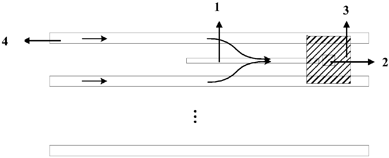
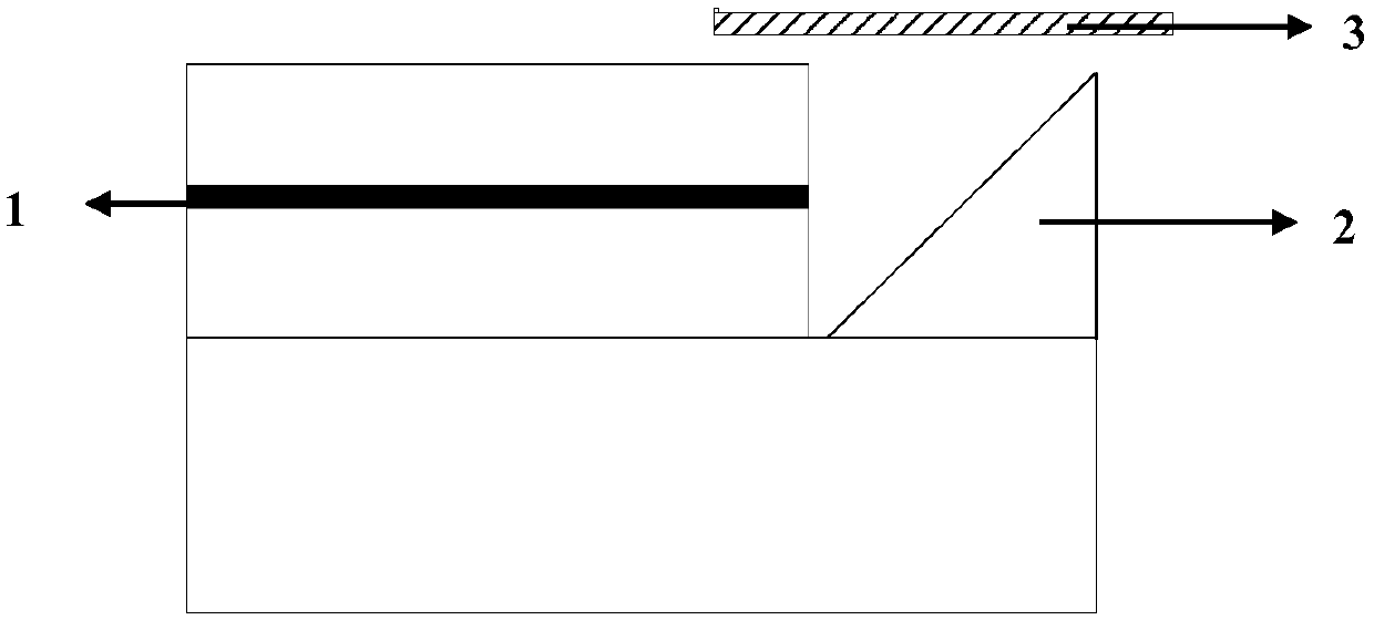
[0034] figure 1 and figure 2 A phase difference measuring device of a waveguide array provided by the present invention is shown, including a monitoring waveguide, an off-chip coupler 2 and a detector 3; the monitoring waveguide is arranged between adjacent array waveguides 4, and the array waveguide 4 A coupled light beam is formed through evanescent wave coupling; the coupled light beam is transmitted to the detector 3 through the off-chip coupler 2; the detector 3 converts the coupled light beam and outputs a current signal. The detector 3 is arranged at the end of the monitoring waveguide. The integrated optical chip is a silicon-based SOI chip, the core material of the arrayed waveguide 4 is monocrystalline silicon, the thickness is 220nm, the width is 450nm, and the waveguide spacing is 2um; the monitoring waveguide width is 450nm, the length is 100um, and the coupling ratio between the monitoring waveguide and the arrayed waveguide 4 is - 23dB; the end of the monitor...

Embodiment 2

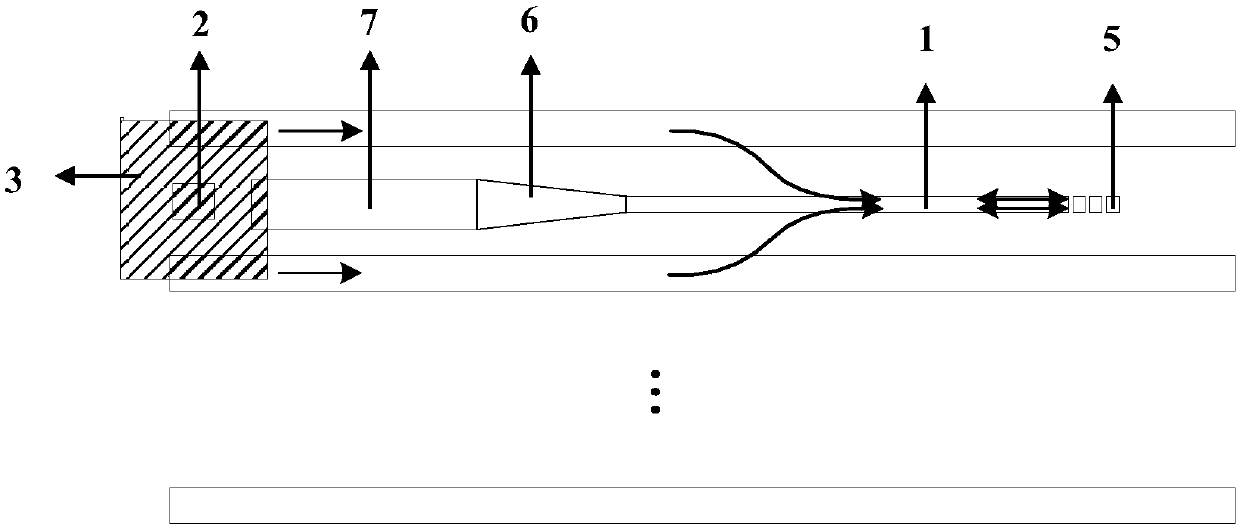
[0038] A method for measuring phase difference of a waveguide array, comprising: coupling between adjacent array waveguides 4 and monitoring waveguides through evanescent wave coupling to form coupled light beams; measuring the total power of the coupled light beams; obtaining the phase difference through the cosine relationship between the total power and the phase difference . The monitoring waveguide and the array waveguide 4 are coupled by evanescent waves, and part of the light is extracted into the monitoring waveguide. A part of the light in the two adjacent waveguides is coupled into the monitoring waveguide, and the two parts of the light are coherently superimposed, and the total power and the phase difference between the two parts of the light have a cosine relationship. When the phase difference is 0, the power reaches the maximum value; when the phase difference is 180 degrees, the power reaches the minimum value.


PUM


Abstract

The invention provides a phase difference measurement device for a waveguide array. The device comprises a monitoring waveguide, an off-chip coupler and a detector, wherein the monitoring waveguide isdisposed between adjacent array waveguides; a coupled light beam is formed between the monitoring waveguide and the array waveguides through an evanescent wave; the coupled light beam is transmittedto the detector through the off-chip coupler; and the detector converts the coupled light beam and outputs a current signal. The power extraction and beam combination are realized through a single waveguide; the interference power is measured by the detector; the structure is compact; and the device is conveniently disposed at the output end of a phased array chip or near an antenna to achieve accurate phase difference measurement.

Description

technical field [0001] The invention relates to the technical field of waveguide arrays, in particular to a phase difference measurement device and a measurement method for waveguide arrays. Background technique [0002] The output beam scanning of the phased array chip is realized by dynamically adjusting the phase difference between the array waveguides. The phase difference is determined by three factors: the wavelength of the input light, the effective refractive index of the waveguide, and the length of the waveguide. The modulation of the phase difference can be realized by adjusting the effective refractive index of the waveguide, or adjusting the wavelength of the incident light by using a wavelength-tunable laser. [0003] Due to the limitation of chip processing conditions, the initial phase difference between different waveguides in the arrayed waveguide is randomly distributed. Before scanning the beam direction, the phase difference correction needs to be perfor...

Claims


Application Information

Patent Timeline
Patent Type & Authority Applications(China)
IPC IPC(8): G01M11/00
CPCG01M11/00
Inventor 刘敬伟李文玲田立飞张新群
Owner CHINA SCI PHOTON CHIP HAINING TECH CO LTD
Why Eureka
Try Eureka