Semiconductor structure and method of forming same

A semiconductor and pattern layer technology, applied in semiconductor/solid-state device manufacturing, electrical components, circuits, etc., can solve problems such as poor semiconductor structure performance, and achieve the effects of reducing loss, saving process costs, and simplifying process flow

Active Publication Date: 2019-04-02
SEMICON MFG INT (SHANGHAI) CORP +1
View PDF4 Cites 1 Cited by
  • Summary
  • Abstract
  • Description
  • Claims
  • Application Information

AI Technical Summary

Problems solved by technology

[0004] With the improvement of the integration of semiconductor devices, when the density of patterns in different regions on the same chip is different, the performance of the semiconductor structure formed by the double patterning process is poor

Method used


Image

  • Semiconductor structure and method of forming same
  • Semiconductor structure and method of forming same
  • Semiconductor structure and method of forming same

Examples


Embodiment Construction

[0036] There are many problems in the method of forming the semiconductor structure, for example, the performance of the formed semiconductor structure is poor.

[0037] In combination with the formation method of the semiconductor structure, the reasons for the poor performance of the formed semiconductor structure are analyzed:

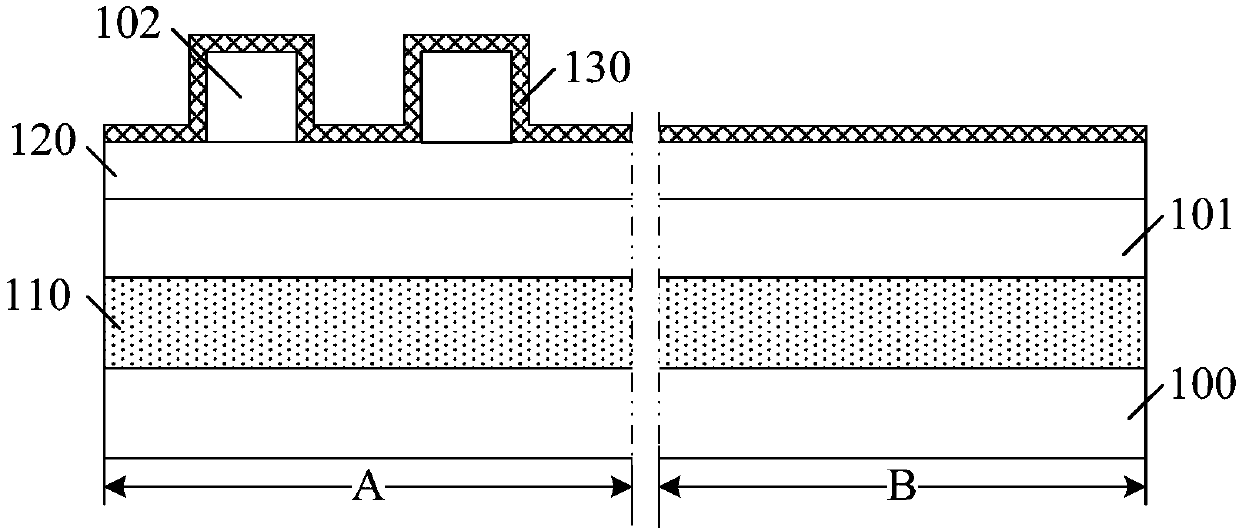
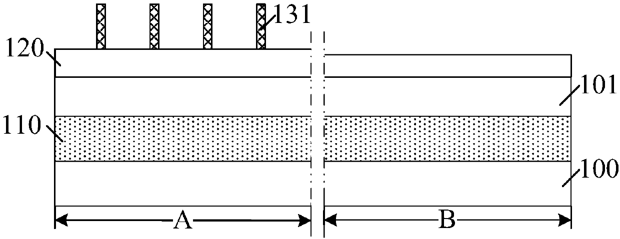
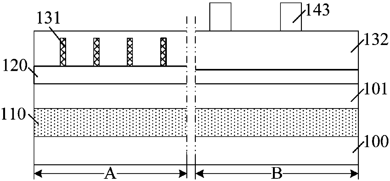
[0038] A substrate is provided, the substrate includes a first region and a second region; a dummy gate layer is formed on the substrate in the first region and the second region; a plurality of discrete first gate layers are formed on the dummy gate layer A pattern layer; a second pattern layer is formed on the dummy gate layer in the second region; the distance between the centers of adjacent second pattern layers is greater than or equal to twice the distance between adjacent first pattern layers; The first pattern layer and the second pattern layer are used as masks to etch the dummy gate layer to form a dummy gate.

[0039] Wherein, in order t...


PUM

PropertyMeasurementUnit
Sizeaaaaaaaaaa

Abstract

The present invention provides a semiconductor structure and a method of forming the same. The method includes the steps of: forming an initial functional layer on a substrate in a first region and ina second region; forming an initial mask layer on the initial functional layer; forming a plurality of separated graphic layers on the initial mask layer in the first region, and forming second graphic layers on the initial mask layer in a removal region and a remaining region, wherein the dimension of the first graphic layer is a first dimension in a first direction, the dimension of the secondgraphic layer is a second dimension in the first direction, the second dimension is equal to the first dimension, and the distance between the first graphic layers is equal to the distance between theadjacent second graphic layers; performing graph transfer processing to form a plurality of mask layers. The forming method provided by the invention can improve the performances of the formed semiconductor structure and can simplify the process flow.

Description

technical field [0001] The invention relates to the technical field of semiconductor manufacturing, in particular to a semiconductor structure and a forming method thereof. Background technique [0002] With the rapid development of semiconductor manufacturing technology, semiconductor devices are developing in the direction of high density and high integration. In order to reduce the size of semiconductor devices and improve the integration of semiconductor devices, multiple patterning processes have been developed in the prior art, including double patterning processes, triple patterning processes and quadruple patterning processes. [0003] The double patterning process can effectively reduce the difficulty of making small-size graphics, and has important applications in forming small-size graphics. The double patterning process includes self-aligned double exposure (SADP) technology, double etching double patterning (DEDP) technology and single etching double patterning...

Claims


Application Information

Patent Timeline
IPC IPC(8): H01L21/027H01L21/033H01L21/8234
CPCH01L21/0271H01L21/0274H01L21/0332H01L21/823437
Inventor 陈卓凡王彦张海洋
Owner SEMICON MFG INT (SHANGHAI) CORP
Why Eureka
Try Eureka