Supercharge Your Innovation With Domain-Expert AI Agents!

Surface defect inspection with large particle monitoring and laser power control

一种表面检验、功率控制的技术,应用在测量装置、半导体/固态器件制造、通过光学手段进行材料分析等方向,能够解决光束功率损失、缺陷检测敏感度、损失等问题

Active Publication Date: 2019-04-02
KLA CORP
View PDF8 Cites 0 Cited by
  • Summary
  • Abstract
  • Description
  • Claims
  • Application Information

AI Technical Summary

Problems solved by technology

In typical bare wafer applications where shot noise is limited, loss of overall beam power results in loss of defect detection sensitivity

Method used


Image

  • Surface defect inspection with large particle monitoring and laser power control
  • Surface defect inspection with large particle monitoring and laser power control
  • Surface defect inspection with large particle monitoring and laser power control

Examples


Embodiment Construction

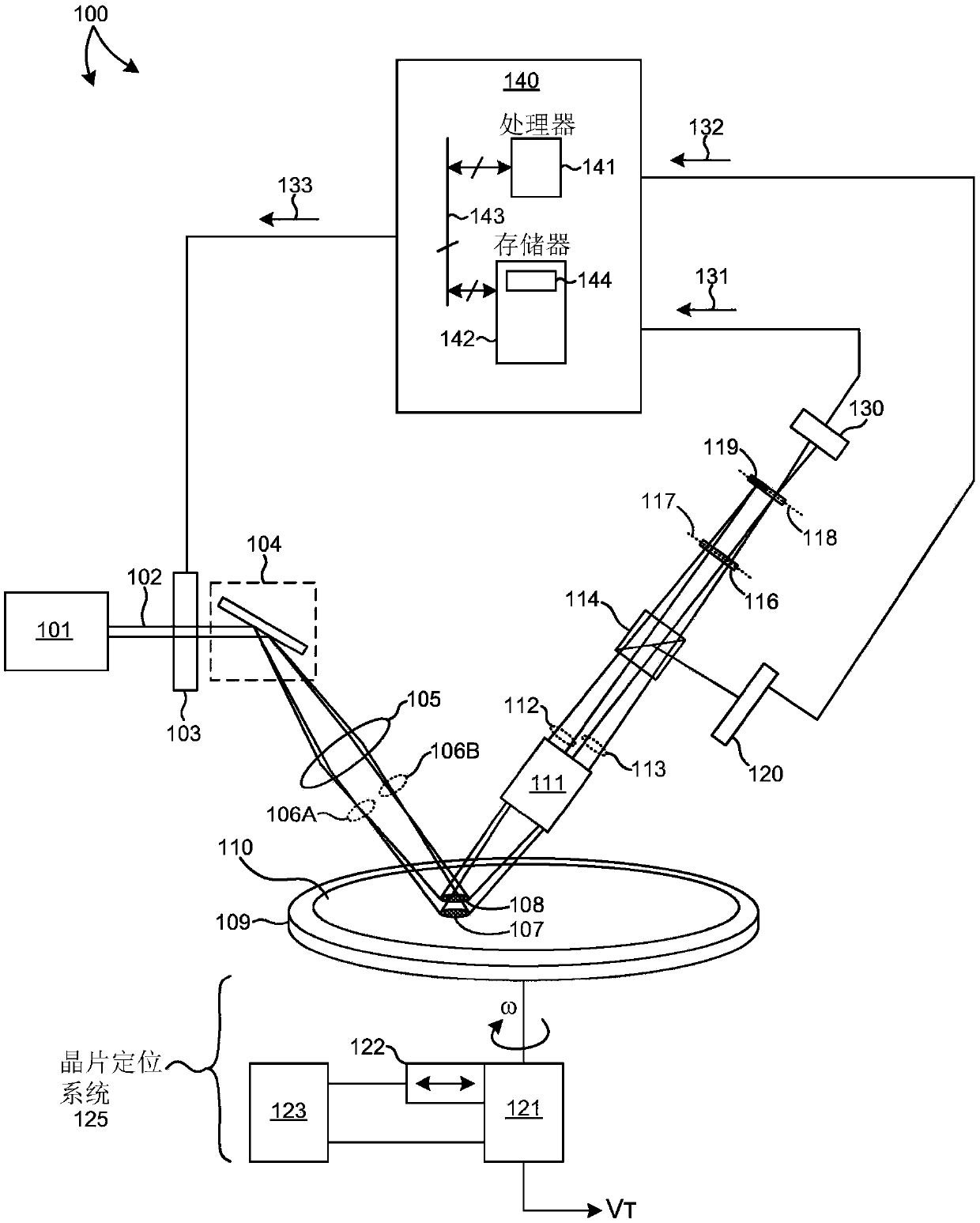
[0029] Reference will now be made in detail to background examples and some embodiments of the invention, examples of which are illustrated in the accompanying drawings.

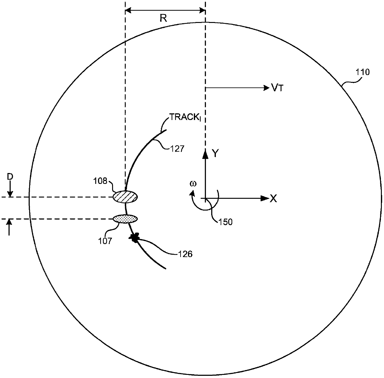
[0030] The inventive concepts described herein are based on the observation that larger particles (eg, particles larger than microns in diameter) are more likely to be damaged by an incident laser beam than smaller particles. For example, larger particles have a greater surface area and, thus, tend to absorb significantly more power than smaller particles with a smaller surface area. Larger particles also tend to scatter significantly more light than smaller particles due to greater surface area and / or increased surface irregularities. For example, the relative amount of light scattered from a particle of radius R is proportional to the sixth power of the particle's radius. Take advantage of the tendency of large particles to strongly scatter light to reduce thermal damage during surface inspection.

[003...


PUM


Abstract

Methods and systems for reducing illumination intensity while scanning over large particles are presented herein. A surface inspection system determines the presence of a large particle in the inspection path of a primary measurement spot using a separate leading measurement spot. The inspection system reduces the incident illumination power while the large particle is within the primary measurement spot. The primary measurement spot and the leading measurement spot are separately imaged by a common imaging collection objective onto one or more detectors. The imaging based collection design spatially separates the image of the leading measurement spot from the image of the primary measurement spot at one or more wafer image planes. Light detected from the leading measurement spot is analyzed to determine a reduced power time interval when the optical power of the primary illumination beam and the leading illumination beam are reduced.

Description

technical field [0001] The described embodiments relate to systems for surface inspection, and more particularly, to semiconductor wafer inspection modalities. Background technique [0002] Semiconductor devices, such as logic and memory devices, are typically fabricated through a series of processing steps applied to a substrate or wafer. Various features and multiple structural levels of the semiconductor device are formed through these processing steps. For example, photolithography, among other things, is a semiconductor manufacturing process that involves creating patterns on semiconductor wafers. Additional examples of semiconductor fabrication processes include, but are not limited to, chemical mechanical polishing, etching, deposition, and ion implantation. Multiple semiconductor devices may be fabricated on a single semiconductor wafer and then separated into individual semiconductor devices. [0003] Inspection processes are used at various steps during the semi...

Claims


Application Information

Patent Timeline
Patent Type & Authority Applications(China)
IPC IPC(8): H01L21/66H01L21/67
CPCG01N21/956G01N21/9501G01N21/8806H01L21/67242H01L22/12H01L22/30
Inventor 史帝夫·宜丰·崔杰(春圣)·黄王春海克里斯堤安·渥特斯布雷特·怀特塞德阿纳托利·罗曼诺夫斯基黄传勇唐纳德·佩蒂伯恩
Owner KLA CORP
Features
  • R&D
  • Intellectual Property
  • Life Sciences
  • Materials
  • Tech Scout
  • Unparalleled Data Quality
  • Higher Quality Content
  • 60% Fewer Hallucinations
Learn More