
A method for improving the qualified rate of indium antimonide cut wafers

An indium antimonide crystal ingot, indium antimonide technology, which is applied to fine working devices, manufacturing tools, stone processing equipment and other directions, can solve the problems of low yield and easy occurrence of fragments, and achieves improved finished products, reduced labor, improved The effect of work efficiency

Active Publication Date: 2021-01-19
云南昆物新跃光电科技有限公司
View PDF6 Cites 0 Cited by
  • Summary
  • Abstract
  • Description
  • Claims
  • Application Information

AI Technical Summary

Problems solved by technology

[0011] However, due to the physical and chemical properties of the indium antimonide material, when cutting with a multi-wire cutting machine, if you do not choose the appropriate equipment and cutting conditions, just fix the bottom of the indium antimonide material on the base of the cutting machine by conventional methods Cutting on the top is prone to fragmentation problems and the yield is low, so there is an urgent need for a method to increase the yield, reduce the breakage rate or eliminate the breakage rate

Method used


Image

  • A method for improving the qualified rate of indium antimonide cut wafers
  • A method for improving the qualified rate of indium antimonide cut wafers

Examples


Embodiment 1

[0026]A method for improving the qualified rate of finished indium antimonide cut wafers, the method steps are as follows:

[0027](1) Place an indium antimonide ingot with a diameter (Ф) of 50mm to be cut on the base of the MWS-610SD multi-filament cutting machine made by Takatori, Japan, and surround the indium antimonide ingot with a baffle. Block, use glue to stick the baffle on the base to form a rectangular parallelepiped frame structure. Only open at the top. Add glue from the opening until the glue fills the gap between the indium antimonide crystal ingot and the baffle. The upper surface of the glue is equal to the height of the indium antimonide crystal ingot to ensure that the surface of the crystal ingot is fully covered by the glue. Place it until the glue is completely solidified and the indium antimonide crystal ingot is fixed on the base of the multi-wire cutting machine;

[0028]According to the diameter and length of the indium antimonide crystal ingot, the baffle is com...

Embodiment 2

[0033]A method for improving the qualified rate of finished indium antimonide cut wafers, the method steps are as follows:

[0034](1) Same as step (1) in the embodiment;

[0035](2) Cut the indium antimonide crystal ingot with a steel wire with a diameter of 0.08mm by a multi-wire cutter at a cutting speed of 4mm / h;

[0036](3) Same as the step (3) of Example 1, a total of 50 indium antimonide wafers were cut, each of which was complete, and the damage rate was zero.


PUM

PropertyMeasurementUnit
Tensile strengthaaaaaaaaaa

Abstract

The invention relates to a method for improving the qualification rate of an indium antimonide cutting wafer finished product, and belongs to the technical field of photoelectric materials. The methodcomprises the steps that an indium antimonide crystal ingot which needs to be cut is placed on a machine base of a multi-wire cutting machine, baffles completely enclose and block the periphery of the indium antimonide crystal ingot, an opening is reserved on the upper part, viscose is added from the opening until the viscose fills a gap between the indium antimonide crystal ingot and the bafflesand the upper surface of the viscose is flush with the indium antimonide crystal ingot, the surface of the indium antimonide crystal ingot is covered with the viscose completely and subjected to placing until the viscose is completely solidified, and the indium antimonide crystal ingot is fixed to the machine base of the multi-wire cutting machine; steel wires with the diameter of 0.08 mm-0.16 mmof the multi-wire cutting machine perform cutting on the indium antimonide crystal ingot at the cutting speed of 4 mm / h-5 mm / h; and the indium antimonide crystal ingot and the machine base are put into a container containing cold water together and heated until the viscose is softened, and cut indium antimonide wafers are taken out from the machine base. According to the method for improving thequalification rate of the indium antimonide cutting wafer finished product, the rate of the finished product is greatly improved, the number of the wafers is increased by over 30%, the labor is reduced, and the economic benefits are improved.

Description

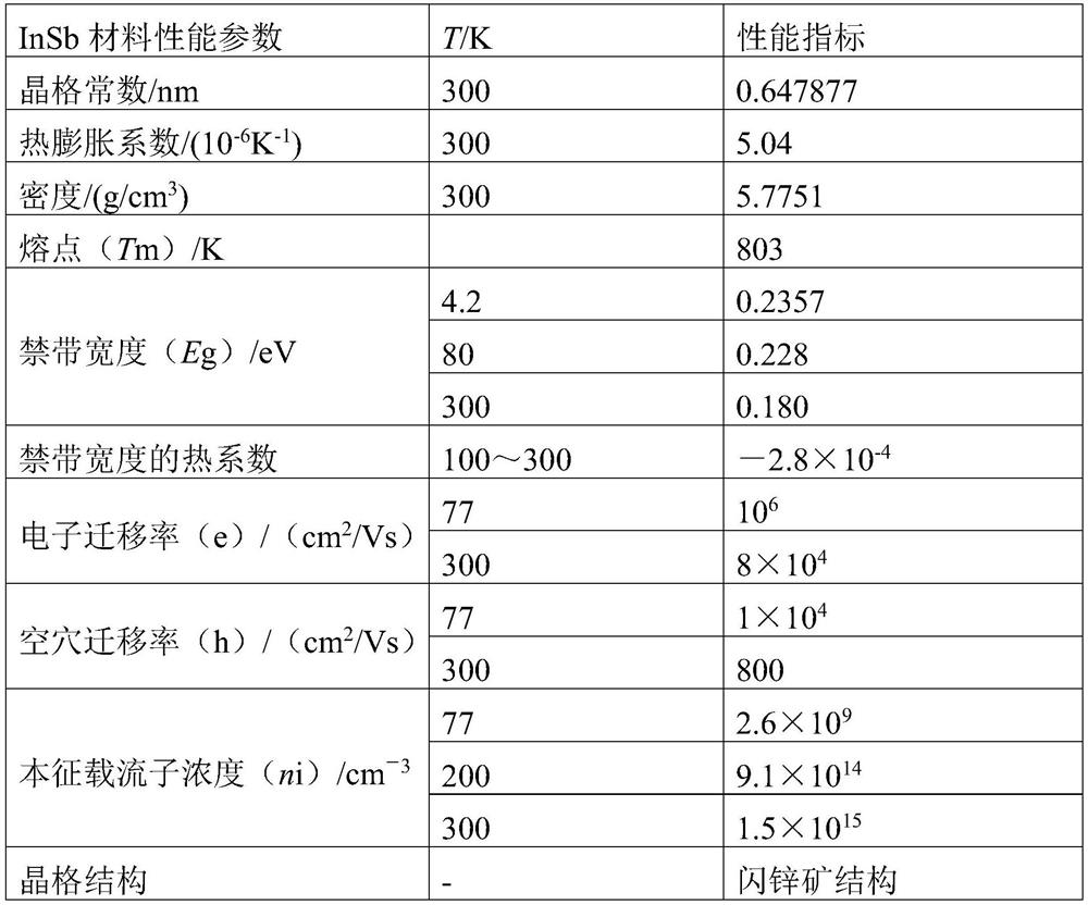
Technical field[0001]The invention relates to a method for improving the qualified rate of finished products of indium antimonide cut wafers, and belongs to the technical field of optoelectronic materials.Background technique[0002]Indium antimonide (InSb) is a III-V compound semiconductor, which has the characteristics of narrow band gap and high mobility. Table 1 lists the basic characteristics of indium antimonide materials. Indium antimonide material has high sensitivity in the infrared band, and is suitable for making mid-wave infrared photodetectors, Hall devices and magnetoresistive elements. In recent years, infrared photodetectors prepared with them have been widely used in infrared tracking systems, infrared cameras, infrared thermal imaging cameras, automatic controllers, gas analyzers, and infrared thermometers.[0003]Table 1 Basic characteristics of indium antimonide materials[0004][0005][0006]The quantum efficiency of infrared detectors is closely related to the selected...

Claims


Application Information

Patent Timeline
Patent Type & Authority Patents(China)
IPC IPC(8): B28D5/04B28D7/00
CPCB28D5/042B28D7/00
Inventor 叶薇陈建才李忠良刘世能何雯瑾太云见赵鹏黄晖
Owner 云南昆物新跃光电科技有限公司
Learn More