Performance test device based on anti-ferroelectric material
A test device and anti-ferroelectric technology, applied in the field of circuits, can solve the problems affecting the use effect, frequency hopping, attenuation, etc. sexual effect
- Summary
- Abstract
- Description
- Claims
- Application Information
AI Technical Summary
Problems solved by technology
Method used
Image
Examples
Embodiment 1
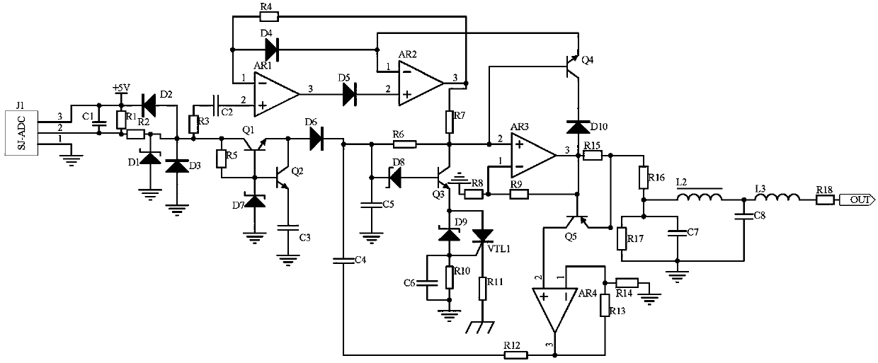
[0012] Embodiment 1, a performance testing device based on antiferroelectric materials, including a signal frequency acquisition circuit, a detection and calibration circuit, and a filter compensation circuit, the signal frequency acquisition circuit uses a signal frequency collector J1 model SJ-ADC to collect data based on antiferroelectric In the electrical material performance testing device, the frequency of the data signal received by the terminal is controlled, and the clamp circuit composed of diode D2 and diode D3 is used to clamp the signal within 0-+5V. The detection and calibration circuit is divided into two circuits to receive the signal frequency acquisition circuit For the output signal, the capacitor C2 is used to filter out the noise of the low-frequency signal, and the peak signal is filtered out by the detection circuit composed of the operational amplifier AR1 and the operational amplifier AR2. At the same time, the triode Q2 and capacitor C3 are used to fil...
Embodiment 2
[0015] Embodiment 2, on the basis of Embodiment 1, the filter compensation circuit uses the inductance L2, the resistor R17, the capacitor C7, and the capacitor C8 to form the clutter in the output signal of the filter circuit and output it to filter out the clutter in the signal, and also That is to compensate the data signal potential received by the control terminal in the performance test device based on antiferroelectric materials to prevent signal attenuation. One end of the inductor L2 is connected to one end of the resistor R16, resistor R17, and capacitor C7, and the other end of the resistor R16 is connected to the transistor Q5. Emitter, the other end of inductor L2 is connected to one end of inductor L3 and one end of capacitor C8, the other end of resistor R17, capacitor C7, and capacitor C8 is grounded, the other end of inductor L3 is connected to one end of resistor R18, and the other end of resistor R18 is connected to the signal output port.
[0016] Implement...
PUM
 Abstract
Description
Claims
Application Information

