Visible light waveband metamaterial perfect absorber and self-assembling preparation method thereof

A perfect absorption and metamaterial technology, applied in the field of visible light band metamaterial perfect absorber and its self-assembly preparation, can solve the problems of low average absorption rate and narrow working bandwidth, and achieve effective regulation of characteristics and stable and reliable self-assembly method. Effect

Active Publication Date: 2019-04-05
INST OF OPTICS & ELECTRONICS - CHINESE ACAD OF SCI
View PDF7 Cites 5 Cited by
  • Summary
  • Abstract
  • Description
  • Claims
  • Application Information

AI Technical Summary

Problems solved by technology

[0005] Aiming at the problems of low average absorption rate and narrow working bandwidth faced by the existing self-assembly method for preparing metamaterial absorbers in the visible light band, the present invention pro

Method used


Image

  • Visible light waveband metamaterial perfect absorber and self-assembling preparation method thereof
  • Visible light waveband metamaterial perfect absorber and self-assembling preparation method thereof
  • Visible light waveband metamaterial perfect absorber and self-assembling preparation method thereof

Examples


Embodiment 1

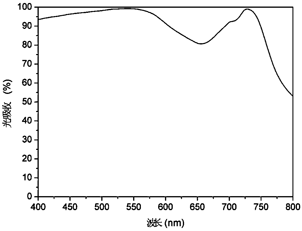
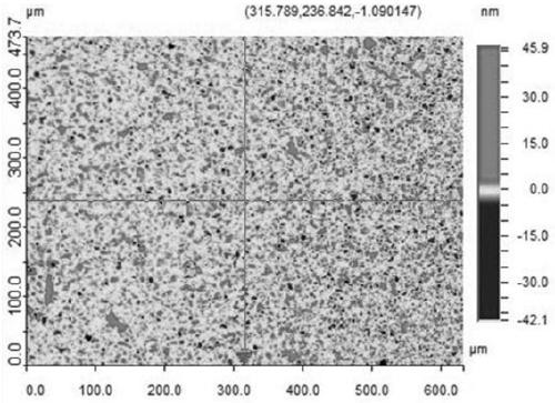
[0019] Place the clean substrate in the vacuum coating system, and plate 80nm thick Al film and 30nm thick SiO from bottom to top respectively. 2 dielectric film, which will subsequently be pre-coated with Al-SiO 2 The film substrate was vertically immersed in a 10mM concentration of positively charged colloidal Aunanoctahedron solution for 36 hours to obtain the upper layer of Au nanoctahedron with a coverage rate of 22%, washed and dried, and finally obtained the desired metamaterial absorber and carried out related structure and performance tests. Test characterization.

Embodiment 2

[0021] Place the clean substrate in a vacuum coating system, and plate a 60nm thick Al film and a 10nm thick SiO film from bottom to top. 2 dielectric film, which will subsequently be pre-coated with Al-SiO 2 The film substrate was vertically immersed in a 10mM concentration of positively charged colloidal Aunanoctahedron solution for 24 hours to obtain the upper layer of Au nanoctahedron with a coverage rate of 17%. After washing and drying, the desired metamaterial absorber was finally obtained and the relevant structures and properties were analyzed. Test characterization.

Embodiment 3

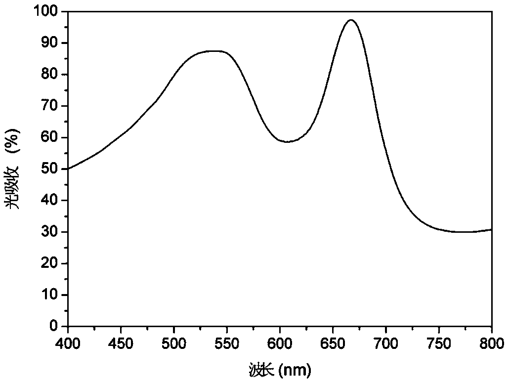
[0023] Place the clean substrate in a vacuum coating system, and plate a 70nm thick Al film and a 50nm thick SiO film from bottom to top. 2 dielectric film, which will subsequently be pre-coated with Al-SiO 2 The film substrate was vertically dipped in a colloidal Aunanoctahedron solution with a positive charge on the surface at a concentration of 10 mM for 60 hours to obtain the upper layer of Au nanoctahedron with a coverage rate of 30%, washed and dried, and finally obtained the desired metamaterial absorber and carried out related structure and performance tests. Test characterization.


PUM


Abstract

The invention discloses a visible light waveband metamaterial perfect absorber and a self-assembling preparation method thereof, and relates to the technical field of functional optical metamaterials.The metamaterial perfect absorber structurally consists of a gold nano octahedral particle upper layer, a silicon dioxide middle medium layer and a metal aluminum bottom layer, and has a membrane thickness of dozens to hundreds nanometers; and the self-assembling process is carried out between mutually electrified nanoparticles and a metal-medium layer under liquid-phase environment. Through controlling each self-assembling test parameters, the prepared metamaterial absorber is capable of realizing an average absorption rate above 80% in a visible light waveband of 400-760 nm; the metamaterial absorber has two typical nearly-perfect absorption peaks at wavelengths close to 540nm and 727nm; the absorption rate is above 99%; and the metamaterial absorber is non-sensitive to incident light polarization.

Description

technical field [0001] The invention relates to the technical field of functional optical metamaterials, in particular to a visible light band metamaterial perfect absorber and a self-assembly preparation method thereof. Background technique [0002] With the rapid development of today's micro-nano science and manufacturing technology, people's regulation of light or electromagnetic waves has reached a new height. Among them, how to realize the effective absorption of light or electromagnetic waves has become one of the key goals in the basic and applied research of functional optical materials. In recent years, a class of metamaterial absorbers formed by sub-wavelength artificial structures of metals and dielectrics has received extensive attention, and has shown significant effects and Huge application potential. [0003] Up to now, people generally use a top-down micro-nano etching processing technology to design the structure of metamaterial absorbers in different work...

Claims


Application Information

Patent Timeline
IPC IPC(8): G02B5/00C23C14/14C23C14/10C23C14/35C23C14/24
CPCC23C14/10C23C14/14C23C14/24C23C14/35G02B5/003
Inventor 张海斌刘红
Owner INST OF OPTICS & ELECTRONICS - CHINESE ACAD OF SCI
Why Eureka
Try Eureka