Semiconductor device and forming method thereof

A semiconductor and device technology, applied in the field of semiconductor devices and their formation, can solve problems such as poor performance of semiconductor devices, and achieve the effects of improving performance and improving current conduction capability.

Inactive Publication Date: 2019-04-05
SEMICON MFG INT (SHANGHAI) CORP +1
View PDF2 Cites 3 Cited by
  • Summary
  • Abstract
  • Description
  • Claims
  • Application Information

AI Technical Summary

Problems solved by technology

[0005] However, the performance of semiconductor devices formed by prior art is poor

Method used


Image

  • Semiconductor device and forming method thereof
  • Semiconductor device and forming method thereof
  • Semiconductor device and forming method thereof

Examples


Embodiment Construction

[0028] As mentioned in the background, semiconductor devices formed in the prior art have poor performance.

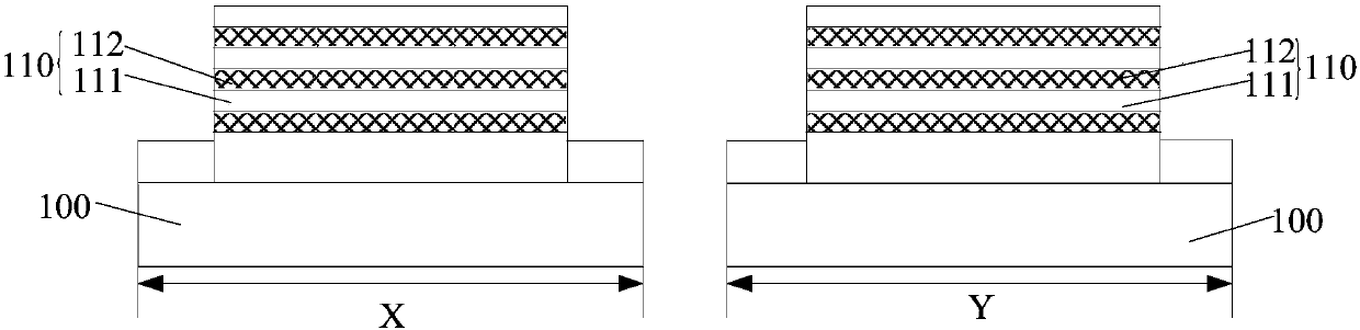
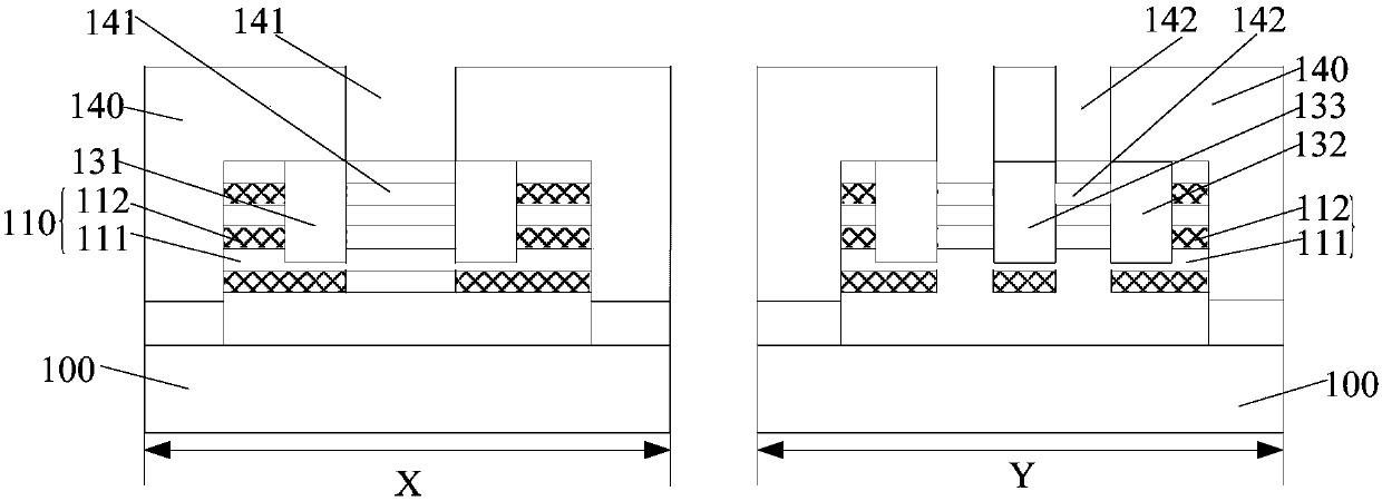
[0029] Figure 1 to Figure 3 It is a structural schematic diagram of the formation process of a semiconductor device.

[0030] refer to figure 1 , providing a semiconductor substrate 100, the semiconductor substrate 100 includes a first region X and a second region Y, the first region X and the second region Y of the semiconductor substrate 100 respectively have fins 110, and the fins 110 are included in the semiconductor substrate Several first fin layers 111 and second fin layers 112 are stacked alternately in the normal direction of the surface of 100 , and the second fin layers 112 are located between adjacent first fin layers 111 .

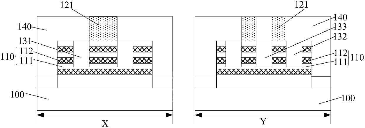
[0031] refer to figure 2 , forming dummy gate structures 121 across the X fins 110 in the first region and the Y fins 110 in the second region respectively; forming source-drain doped layers in the X fins 110 in the first region o...


PUM


Abstract

The invention provides a semiconductor device and a forming method thereof. The method comprises the following steps that a semiconductor substrate is provided, wherein the semiconductor substrate comprises a first region and a second region; fin parts are arranged on the first region and the second region of the semiconductor substrate respectively; the fin parts comprise a plurality of first finpart layers and second fin part layers which are stacked in a staggered mode in the normal direction of the surface of the semiconductor substrate, and the second fin part layers are located betweenthe adjacent first fin part layers; a pseudo gate structure which only spans the fin parts of the first region is formed; a dielectric layer is formed on the first region and the second region of thesemiconductor substrate, and the fin parts in the first region and the fin parts in the second region, wherein the dielectric layer covers the side wall of the pseudo gate structure and exposes the top surface of the pseudo gate structure; then the pseudo gate structure and the second fin part layers covered by the pseudo gate structure are removed; then a first through hole and a second through hole which penetrate through the dielectric layer are formed in the dielectric layer in the second region; a first doping layer is formed in the fin parts at the bottom of the first through hole; and asecond doping layer is formed in the fin parts at the bottom of the second through hole. According to the method, the performance of the semiconductor device is improved.

Description

technical field [0001] The invention relates to the field of semiconductor manufacturing, in particular to a semiconductor device and a forming method thereof. Background technique [0002] MOS transistors are one of the most important components in modern integrated circuits. The basic structure of a MOS transistor includes: a semiconductor substrate; a gate structure located on the surface of the semiconductor substrate; a source region located in the semiconductor substrate on one side of the gate structure; and a drain region located in the semiconductor substrate on the other side of the gate structure. The working principle of the MOS transistor is: by applying a voltage to the gate structure, the current in the channel at the bottom of the gate structure is adjusted to generate a switching signal. [0003] Diode is an important semiconductor device, and diode can be used to form ESD. [0004] Generally, a semiconductor device includes not only MOS transistors but al...

Claims


Application Information

Patent Timeline
Patent Type & Authority Applications(China)
IPC IPC(8): H01L21/8249H01L27/06H01L29/78
CPCH01L21/8249H01L27/0629H01L29/785
Inventor 周飞
Owner SEMICON MFG INT (SHANGHAI) CORP
Why Eureka
Try Eureka