Flexible double-layer threshold value gating tube device and preparation method thereof
A gate and threshold technology, applied in electrical components and other directions, can solve the problems of high deposition temperature of resistive materials, limit flexible memory devices, etc., and achieve improved electrical performance, safe and reliable processes, and reduced requirements and process preparation levels. Effect
- Summary
- Abstract
- Description
- Claims
- Application Information
AI Technical Summary
Problems solved by technology
Method used
Image
Examples
Embodiment 1
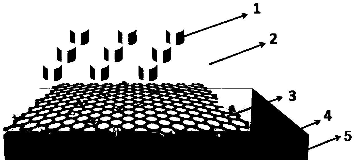
[0039] A flexible double-layer threshold gating tube device in this embodiment, the gating tube device sequentially includes a flexible substrate, a bottom electrode, a graphene oxide film layer, a hafnium oxide film dielectric layer, and a top electrode from bottom to top; wherein: The flexible substrate material is polyethylene naphthalate film (PEN), the bottom electrode is an ITO material, and the top electrode is a Pt material;
[0040] The thickness of the bottom electrode is 200nm, the thickness of the graphene oxide film layer is 40nm, the thickness of the hafnium oxide film layer is 25nm, and the thickness of the top electrode is 150nm;
[0041] The shape of the flexible substrate and the bottom electrode are both square, and the side length of the square is 1.5 cm; the shape of the top electrode is circular, with a diameter of 100 μm.
[0042] The flexible double-layer threshold gate device described above in this embodiment is prepared according to the following met...
Embodiment 2
[0055] A flexible double-layer threshold gating tube device in this embodiment, the gating tube device sequentially includes a flexible substrate, a bottom electrode, a graphene oxide film layer, a hafnium oxide film dielectric layer, and a top electrode from bottom to top; wherein: The flexible substrate material is polyethylene terephthalate (PET), the bottom electrode is an ITO material, and the top electrode is a Pt material;
[0056] The thickness of the bottom electrode is 150nm, the thickness of the graphene oxide film layer is 60nm, the thickness of the hafnium oxide film layer is 25nm, and the thickness of the top electrode is 200nm;
[0057] The shape of the flexible substrate and the bottom electrode are both square, and the side length of the square is 1.5 cm; the shape of the top electrode is circular, with a diameter of 100 μm.
[0058] The flexible double-layer threshold gate device described above in this embodiment is prepared according to the following method...
Embodiment 3
[0067] A flexible double-layer threshold gating tube device in this embodiment, the gating tube device includes a flexible substrate, a bottom electrode, a graphene oxide thin film layer, a hafnium oxide thin film dielectric layer, and a top electrode in sequence from bottom to top; wherein : the flexible substrate material is polyethylene terephthalate (PET), the bottom electrode is an ITO material, and the top electrode is a Pt material;
[0068] The thickness of the bottom electrode is 50nm, the thickness of the graphene oxide film layer is 20nm, the thickness of the hafnium oxide film layer is 20nm, and the thickness of the top electrode is 100nm;
[0069] Both the flexible substrate and the bottom electrode are square in shape with a side length of 1 cm; the top electrode is circular in shape with a diameter of 80 um.
[0070] The flexible double-layer threshold gate device described above in this embodiment is prepared according to the following method, and the method sp...
PUM
| Property | Measurement | Unit |
|---|---|---|
| Thickness | aaaaa | aaaaa |
| Thickness | aaaaa | aaaaa |
| Thickness | aaaaa | aaaaa |
Abstract
Description
Claims
Application Information


