
Method for improving unfavorable board manufacturing at fusing place

A bad and board-making technology, which is applied in the direction of multilayer circuit manufacturing, printed circuit manufacturing, electrical components, etc., can solve the problems of easy delamination, board explosion or surface copper skin blistering, etc., to improve the poor board making of the fusion position , avoid foaming, enhance the binding effect

Inactive Publication Date: 2019-04-05
SHENZHEN SUNTAK MULTILAYER PCB
View PDF7 Cites 4 Cited by
  • Summary
  • Abstract
  • Description
  • Claims
  • Application Information

AI Technical Summary

Problems solved by technology

[0003] The present invention aims at the problem that delamination, cracking or blistering of the surface layer of copper skin tends to occur at the fusion position in the existing pre-fixed PCB production method by fusion, and provides a method that can avoid delamination, cracking or blistering at the fusion position. The method of improving the poor plate making of the fusion position by foaming the surface copper skin

Method used


Image

  • Method for improving unfavorable board manufacturing at fusing place
  • Method for improving unfavorable board manufacturing at fusing place
  • Method for improving unfavorable board manufacturing at fusing place

Examples


Embodiment 1

[0027] This embodiment provides a method for making a rigid-flex board, and in particular provides a method for pre-fixing fusion with fusion technology in the pressing process to improve poor board production due to delamination and explosion at the fusion site.

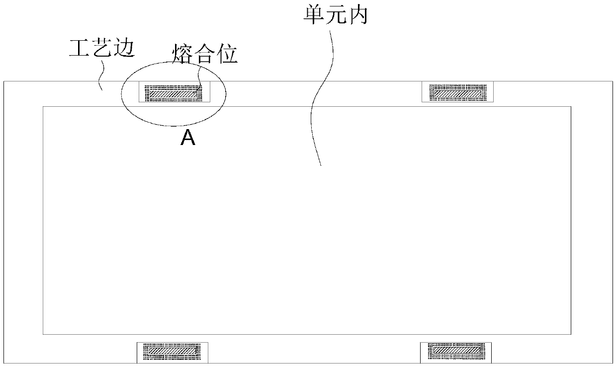
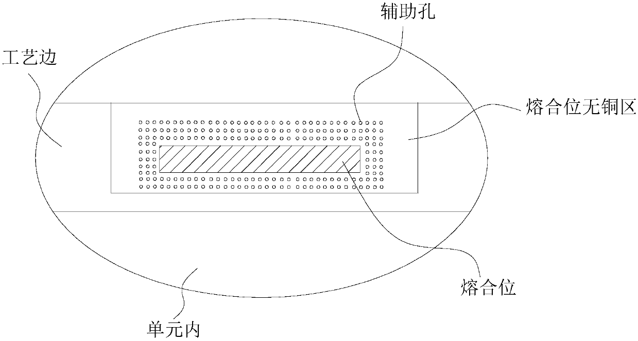
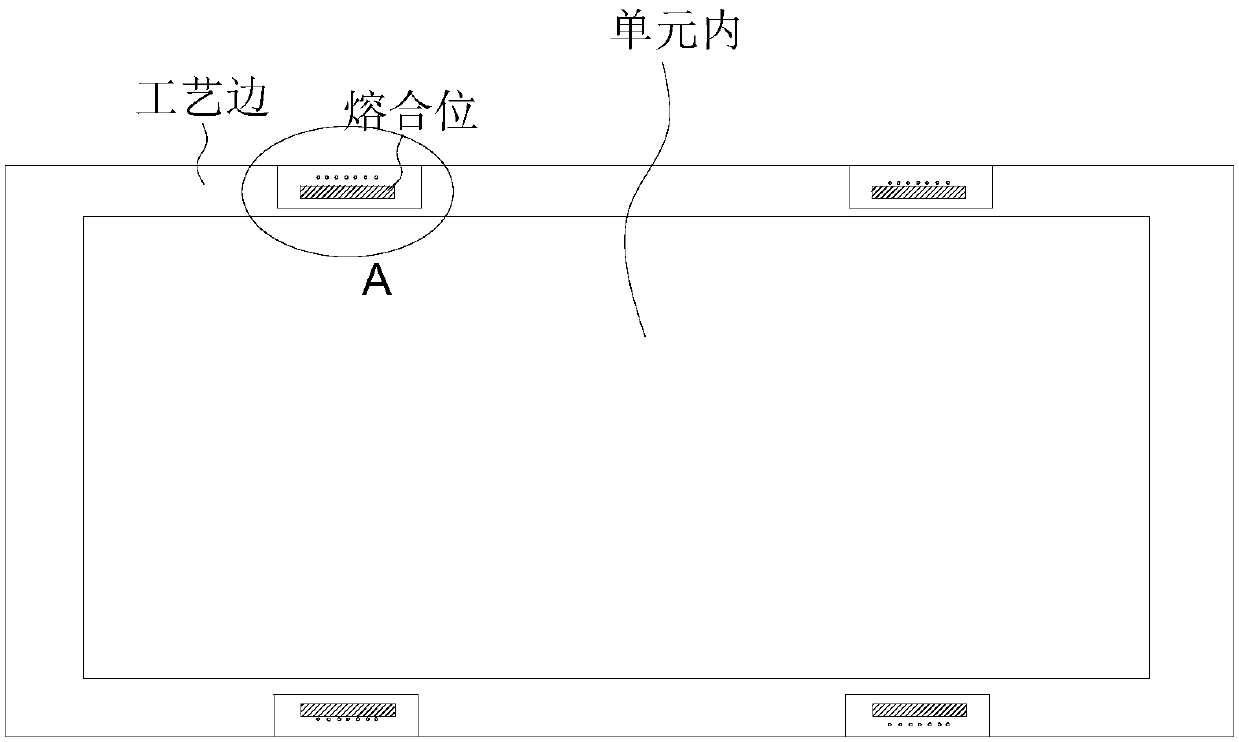
[0028] (1) Cutting: According to the size of the panel required by the design, the core board of the soft board and the core board of the hard board are cut out. The outer periphery of the soft board core board and the hard board core board is the process edge, and the width of the process edge is 25mm.

[0029] (2) Inner layer circuit production (negative film process): Inner layer graphic transfer, use a vertical coating machine to coat photosensitive film, the thickness of the photosensitive film is controlled to 8 μm, use a fully automatic exposure machine, and use a 5-6 grid exposure ruler (21 grid exposure ruler) to complete the exposure of the inner layer circuit; inner layer etching, etch the inner layer cir...

Embodiment 2

[0056] This embodiment provides a method for manufacturing a PCB, and in particular provides a method for pre-fixing fusion with fusion technology in the lamination process to improve poor board production caused by delamination and explosion at the fusion position.

[0057] (1) Cutting: cut out the inner core board according to the panel size required by the design.

[0058] (2) Make the inner layer circuit: adopt the negative process to make the inner layer circuit on the inner layer core board to obtain the inner layer circuit board. After the inner layer circuit is etched on the inner core board, POE punching and inner layer AOI are performed sequentially according to the conventional procedures.

[0059] (3) Lamination: pre-stack the inner core board, prepreg PP, and outer copper foil, and perform fusion pre-fixation by fusion, and pre-fix each layer to form a pre-stacked structure. Then select appropriate lamination conditions according to the Tg of the sheet to press t...


PUM


Abstract

The invention relates to the technical field of circuit board production, in particular to a method for improving unfavorable board manufacturing at a fusing place. An auxiliary hole is formed in a copper-free region of the fusing place, the auxiliary hole with a certain hole diameter size still can be maintained to be a non-metal through hole due to copper deposition and electroplating capabilitylimitation in PCB production, thus, moisture of the fusing place can be permeated during wet processing by cooling and evaporation of the auxiliary hole, and the problems of layering and board explosion are prevented; or the auxiliary hole is formed in the copper-free region of the fusing place, the auxiliary hole with the certain hole diameter size becomes the metal through hole due to subsequent copper deposition and electroplating flow, a copper plating layer formed at the copper-free region of the fusing place is connected with a copper plating layer on the auxiliary hole during the subsequent electroplating process, the binding force between the copper plating layer and a substrate can be improved, so that the problem of bubbles of a surface copper layer at the fusing place can be prevented.

Description

technical field [0001] The invention relates to the technical field of circuit board production, in particular to a method for improving poor plate making at fusion joints. Background technique [0002] The production process of general circuit boards (PCB) mainly includes cutting, inner layer circuit making, pressing, outer layer drilling, copper sinking, outer layer circuit making, solder mask making, surface treatment, molding and other processes. In the pressing process, it is necessary to press the inner core board, the outer layer copper foil / outer core board through the prepreg to form a multi-layer production board, and before pressing, it needs to be welded, riveted or a combination of fusion and riveting. The way to do pre-fixation of each layer. The fusion period of the existing fusion pre-fixing method is generally 100-240 seconds. In such a short fusion period, it is difficult for the prepreg to be completely solidified. In the subsequent wet process, for certa...

Claims


Application Information

Patent Timeline
Patent Type & Authority Applications(China)
IPC IPC(8): H05K3/46
CPCH05K3/4691
Inventor 邓辉季辉卿恒冯涛张小明孙保玉
Owner SHENZHEN SUNTAK MULTILAYER PCB
Features
  • Generate Ideas
  • Intellectual Property
  • Life Sciences
  • Materials
  • Tech Scout
  • Unparalleled Data Quality
  • Higher Quality Content
  • 60% Fewer Hallucinations
Learn More